
我們重視您的隱私
通過點擊「允許所有 Cookie」,代表您同意在您的設備上存儲 Cookie 以增強網站瀏覽體驗、分析網站使用情況並協助我們的行銷和網站效能優化工作。您可以在我們的隱私權政策中找到有關於此的更多資訊。

 - WEO012864D")
 - WEO012864D")
 - WEO012864D")
 - WEO012864D")
 - WEO012864D")
 - WEO012864D")
 - WEO012864D")
 - WEO012864D")
 - WEO012864D")
 - WEO012864D")
 - WEO012864D")
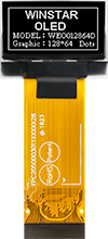
WEO012864D 為華凌光電 (WINSTAR) 最受歡迎的 0.96 吋 COG OLED 顯示器模組,擁有 128x64 解析度並內建 SSD1306 驅動 IC。作為一款技術成熟且被廣泛採用的顯示模組,它具備卓越的穩定性與高相容性,適用於各類工業控制及消費性電子產品。
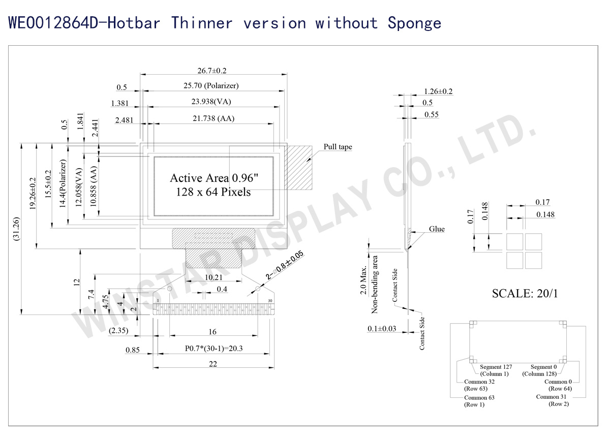
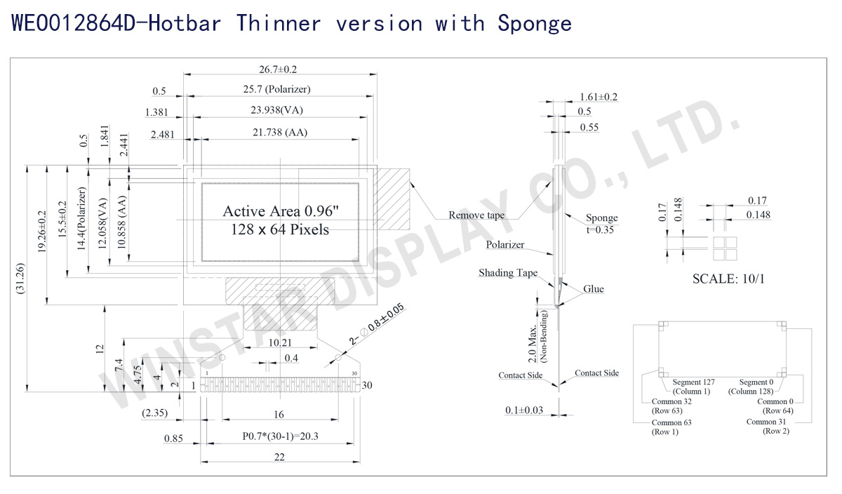
WEO012864D 系列提供兩種厚度規格,兩者具備完全相同的電氣特性與針腳定義 (Pin Assignment):

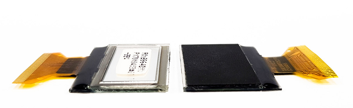
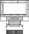
圖左: 標準輕薄版 (1.26mm) | 圖右: 加海綿超薄版 (可相容 1.61mm 規格)
| 項目 | WEO012864D-Hotbar | WEO012864D-Hotbar 含Sponge泡棉 | 單位 |
|---|---|---|---|
| 點陣 | 128 × 64 | Dots | |
| 模組尺寸 | 26.7 × 19.26 × 1.26 | 26.7 × 19.26 × 1.61 | mm |
| 有效區域 | 21.738 × 10.858 | mm | |
| 點大小 | 0.148 × 0.148 | mm | |
| 點間距 | 0.17 × 0.17 | mm | |
| 顯示模式 | 被動矩陣 | ||
| 發光顏色 | 單色 | ||
| 驅動方式 | 1/64 Duty | ||
| IC | SSD1306 | ||
| 介面 | 6800,8080,SPI,I2C | ||
| 尺寸 | 0.96 吋 | ||
| 參數 | 符號 | 最小值 | 最大值 | 單位 |
|---|---|---|---|---|
| 邏輯電源電壓 | VDD | 0 | 4.0 | V |
| 顯示電源電壓 | VCC | 0 | 15.0 | V |
| 工作溫度 | TOP | -40 | +80 | °C |
| 儲存溫度 | TSTG | -40 | +85 | °C |
| 項目 | 符號 | 條件 | 最小值 | 典型值 | 最大值 | 單位 |
|---|---|---|---|---|---|---|
| 邏輯電源供應 | VDD | - | 2.8 | 3.0 | 3.3 | V |
| 顯示電源供應 | VCC | - | 11.5 | 12.0 | 12.5 | V |
| 輸入高電壓 | VIH | - | 0.8×VDD | - | VDDIO | V |
| 輸入低電壓 | VIL | - | 0 | - | 0.2×VDD | V |
| 輸出高電壓 | VOH | - | 0.9×VDD | - | VDDIO | V |
| 輸出低電壓 | VOL | - | 0 | - | 0.1×VDD | V |
| Operating Current for VCC (50% display ON) | ICC | - | - | 16.0 | 20.0 | mA |
| No. | 符號 | 說明 |
|---|---|---|
| 1 | N.C. (GND) | Reserved Pin (Supporting Pin) The supporting pins can reduce the influences from stresses on the function pins. These pins must be connected to external ground. |
| 2 | C2N | Positive Terminal of the Flying Inverting Capacitor Negative Terminal of the Flying Boost Capacitor The charge-pump capacitors are required between the terminals. They must be floated when the converter is not used. |
| 3 | C2P | |
| 4 | C1P | |
| 5 | C1N | |
| 6 | VBAT | Power Supply for DC/DC Converter Circuit This is the power supply pin for the internal buffer of the DC/DC voltage converter. It must be connected to external source when the converter is used. It should be connected to VDD when the converter is not used. |
| 7 | NC | NC |
| 8 | VSS | Ground of Logic Circuit This is a ground pin. It acts as a reference for the logic pins. It must be connected to external ground. |
| 9 | VDD | Power Supply for Logic This is a voltage supply pin. It must be connected to external source. |
| 10 | BS0 | Communicating Protocol Select These pins are MCU interface selection input. See the following table: 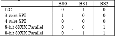 |
| 11 | BS1 | |
| 12 | BS2 | |
| 13 | CS# | Chip Select This pin is the chip select input. The chip is enabled for MCU communication only when CS# is pulled low. |
| 14 | RES# | Power Reset for Controller and Driver This pin is reset signal input. When the pin is low, initialization of the chip is executed. |
| 15 | D/C# | Data/Command Control This pin is Data/Command control pin. When the pin is pulled high, the input at D7~D0 is treated as display data. When the pin is pulled low, the input at D7~D0 will be transferred to the command register. For detail relationship to MCU interface signals, please refer to the Timing Characteristics Diagrams. When the pin is pulled high and serial interface mode is selected, the data at SDIN is treated as data. When it is pulled low, the data at SDIN will be transferred to the command register. In I2C mode, this pin acts as SA0 for slave address selection. |
| 16 | R/W# | Read/Write Select or Write This pin is MCU interface input. When interfacing to a 68XX-series microprocessor, this pin will be used as Read/Write (R/W#) selection input. Pull this pin to “High” for read mode and pull it to “Low” for write mode. When 80XX interface mode is selected, this pin will be the Write (WR#) input. Data write operation is initiated when this pin is pulled low and the CS# is pulled low. |
| 17 | E/RD# | Read/Write Enable or Read This pin is MCU interface input. When interfacing to a 68XX-series microprocessor, this pin will be used as the Enable (E) signal. Read/write operation is initiated when this pin is pulled high and the CS# is pulled low. When connecting to an 80XX-microprocessor, this pin receives the Read (RD#) signal. Data read operation is initiated when this pin is pulled low and CS# is pulled low. |
| 18~25 | D0~D7 | Host Data Input/Output Bus These pins are 8-bit bi-directional data bus to be connected to the microprocessor's data bus. When serial mode is selected, D1 will be the serial data input SDIN and D0 will be the serial clock input SCLK. When I2C mode is selected, D2 & D1 should be tired together and serve as SDAout & SDAin in application and D0 is the serial clock input SCL. |
| 26 | IREF | Current Reference for Brightness Adjustment This pin is segment current reference pin. A resistor should be connected between this pin and VSS. Set the current lower than 12.5μA. |
| 27 | VCOMH | Voltage Output High Level for COM Signal This pin is the input pin for the voltage output high level for COM signals. A capacitor should be connected between this pin and VSS. |
| 28 | VCC | Power Supply for OEL Panel This is the most positive voltage supply pin of the chip. A stabilization capacitor should be connected between this pin and VSS when the converter is used. It must be connected to external source when the converter is not used. |
| 29 | VLSS | Ground of Analog Circuit This is an analog ground pin. It should be connected to VSS externally. |
| 30 | NC (GND) |
Reserved Pin (Supporting Pin) The supporting pins can reduce the influences from stresses on the function pins. These pins must be connected to external ground. |
| Drawing | FPC Length | PIN | Pitch | ZIF FPC or HOTBAR FPC | Interface | FPC No. | Create Date |
|---|---|---|---|---|---|---|---|
 |
22 | 30 | 0.7 | HOTBAR | 6800,8080,SPI,I2C | FPC2070003001XXXXX08 | 20170808 |
 |
41.1 | 30 | 0.5 | ZIF | 6800,8080,SPI,I2C | FPC2050003011XXXXX28 | 20180604 |
 |
13.1 | 30 | 0.5 | ZIF | 6800,8080,SPI,I2C | FPC2050003011XXXXX34 | 20200221 |

通過點擊「允許所有 Cookie」,代表您同意在您的設備上存儲 Cookie 以增強網站瀏覽體驗、分析網站使用情況並協助我們的行銷和網站效能優化工作。您可以在我們的隱私權政策中找到有關於此的更多資訊。