
我們重視您的隱私
通過點擊「允許所有 Cookie」,代表您同意在您的設備上存儲 Cookie 以增強網站瀏覽體驗、分析網站使用情況並協助我們的行銷和網站效能優化工作。您可以在我們的隱私權政策中找到有關於此的更多資訊。

 - WEO012864C")
 - WEO012864C")
 - WEO012864C")
 - WEO012864C")
 - WEO012864C")
 - WEO012864C")
 - WEO012864C")
 - WEO012864C")
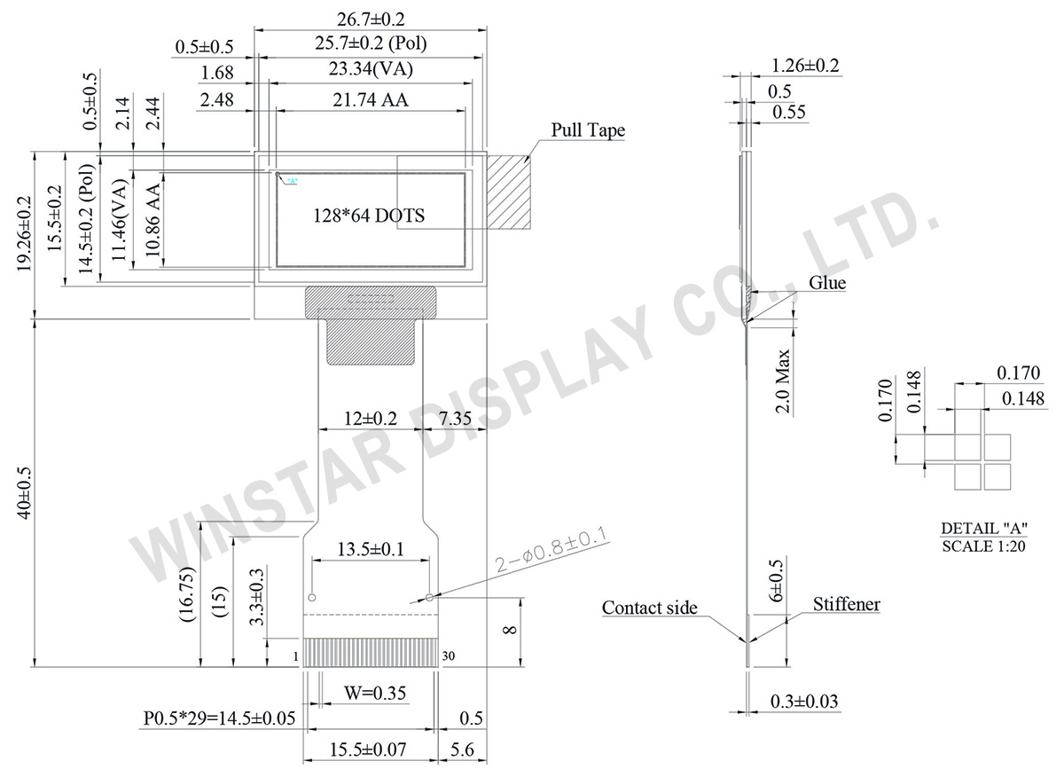
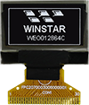
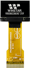
WEO012864C 是一款高性能的 0.96 吋 128x64 COG (Chip on Glass) OLED 顯示模組,內建 SH1106 控制 IC。其 0.96 吋 OLED 模組外觀尺寸僅 26.70 x 19.26 mm,專為空間受限的應用所設計,是 IoT 終端、手持式產品, 量測儀表/儀器、穿戴式裝置及工業儀器的理想選擇。
憑藉堅固的 COG 結構與靈活的硬體配置選項,WEO012864C 0.96 吋 OLED 模組 讓研發團隊能為特定專業應用選擇最優化的硬體設定。
 可選 FPC
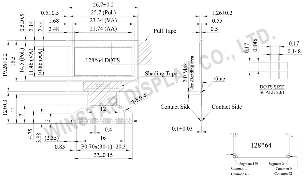
| 項目 | 規格 | 單位 |
|---|---|---|
| 點陣(解析度) | 128 x 64 | - |
| 模組尺寸 | 26.70 × 19.26 ×1.26 | mm |
| 有效區域 | 21.74 × 10.86 | mm |
| 點大小 | 0.148 × 0.148 | mm |
| 點間距 | 0.170 × 0.170 | mm |
| 顯示模式 | 被動矩陣 | |
| 發光顏色 | 單色 | |
| 驅動方式 | 1/64 Duty | |
| 控制器IC | SH1106 | |
| 介面 | 6800, 8080, SPI, I2C | |
| 尺寸 | 0.96 吋 | |
| 參數 | 符號 | 最小值 | 最大值 | 單位 |
|---|---|---|---|---|
| 邏輯電源電壓 | VDD1 | -0.3 | 3.6 | V |
| 電荷幫浦電源 | VDD2 | -0.3 | 4.8 | V |
| 顯示電源電壓 | VPP | -0.3 | 14.5 | V |
| 工作溫度 | TOP | -40 | +80 | °C |
| 儲存溫度 | TSTG | -40 | +85 | °C |
| 項目 | 符號 | 條件 | 最小值 | 典型值 | 最大值 | 單位 |
|---|---|---|---|---|---|---|
| 邏輯電源電壓 | VDD1 | - | 2.8 | 3.0 | 3.3 | V |
| 電荷幫浦電源 | VDD2 | - | 3.5 | 3.8 | 4.2 | V |
| 顯示器的電荷幫浦輸出電壓 (Generated by Internal DC/DC) |
Charge Pump VPP |
- | 7.5 | 8 | 8.5 | V |
| 輸入高準位 | VIH | - | 0.8xVDD1 | - | VDD1 | V |
| 輸入低準位 | VIL | - | VSS | - | 0.2xVDD1 | V |
| 輸出高準位 | VOH | - | 0.8xVDD1 | - | VDD1 | V |
| 輸出低準位 | VOL | - | VSS | - | 0.2xVDD1 | V |
| VDD2的工作電流顯示50%ON | IDD2 | - | - | 10 | 16 | mA |
| No. | 符號 | 功能說明 | |||||||||||||||
|---|---|---|---|---|---|---|---|---|---|---|---|---|---|---|---|---|---|
| 1 | NC | No connection | |||||||||||||||
| 2 | C1N | Connect to charge pump capacitor. These pins are not used and should be disconnected when Vpp is supplied externally. |
|||||||||||||||
| 3 | C1P | ||||||||||||||||
| 4 | C2P | Connect to charge pump capacitor. These pins are not used and should be disconnected when Vpp is supplied externally. |
|||||||||||||||
| 5 | C2N | ||||||||||||||||
| 6 | VDD2 | 3.0 – 4.7V power supply pad for Power supply for charge pump circuit. This pin should be disconnected when VPP is supplied externally |
|||||||||||||||
| 7 | NC | No connection | |||||||||||||||
| 8 | VSS | Ground. | |||||||||||||||
| 9 | VDD1 | Power supply input: 1.65 - 3.5V | |||||||||||||||
| 10 | NC | No connection | |||||||||||||||
| 11 | IM1 | These are the MPU interface mode select pads.
|
|||||||||||||||
| 12 | IM2 | ||||||||||||||||
| 13 | CSB | This pad is the chip select input. When CSB = “L”, then the chip select becomes active, and data/command I/O is enabled. | |||||||||||||||
| 14 | RESB | This is a reset signal input pad. When RES is set to “L”, the settings are initialized. The reset operation is performed by the RES signal level. | |||||||||||||||
| 15 | A0 | This is the Data/Command control pad that determines whether the data bits are data or a command. A0 = “H”: the inputs at D0 to D7 are treated as display data. A0 = “L”: the inputs at D0 to D7 are transferred to the command registers. In I2C interface, this pad serves as SA0 to distinguish the different address of OLED driver. |
|||||||||||||||
| 16 | WRB | This is a MPU interface input pad. When connected to an 8080 MPU, this is active LOW. This pad connects to the 8080 MPU WR signal. The signals on the data bus are latched at the rising edge of the WR signal. When connected to a 6800 Series MPU: This is the read/write control signal input terminal. When R/W = “H”: Read. When R/W = “L”: Write. |
|||||||||||||||
| 17 | RDB | This is a MPU interface input pad. When connected to an 8080 series MPU, it is active LOW. This pad is connected to the RD signal of the 8080 series MPU, and the data bus is in an output status when this signal is “L”. When connected to a 6800 series MPU , this is active HIGH. This is used as an enable clock input of the 6800 series MPU. When RD = “H”: Enable. When RD = “L”: Disable. |
|||||||||||||||
| 18 | D0 | This is an 8-bit bi-directional data bus that connects to an 8-bit or 16-bit standard MPU data bus. When the serial interface is selected, then D0 serves as the serial clock input pad (SCL) and D1 serves as the serial data input pad (SI). At this time, D2 to D7 are set to high impedance. When the I2C interface is selected, then D0 serves as the serial clock input pad (SCL) and D1 serves as the serial data input pad (SDAI). At this time, D2 to D7 are set to high impedance. |
|||||||||||||||
| 19 | D1 | ||||||||||||||||
| 20 | D2 | ||||||||||||||||
| 21 | D3 | ||||||||||||||||
| 22 | D4 | ||||||||||||||||
| 23 | D5 | ||||||||||||||||
| 24 | D6 | ||||||||||||||||
| 25 | D7 | ||||||||||||||||
| 26 | IREF | This is a segment current reference pad. A resistor should be connected between this pad and VSS. Set the current at 18.75uA. | |||||||||||||||
| 27 | VCOMH | This is a pad for the voltage output high level for common signals. A capacitor should be connected between this pad and VSS. |
|||||||||||||||
| 28 | VPP | OLED panel power supply. Generated by internal charge pump. Connect to capacitor. It could be supplied externally. |
|||||||||||||||
| 29 | NC | No connection | |||||||||||||||
| 30 | NC | No connection |
| Drawing | FPC Length | PIN | Pitch | ZIF FPC or HOTBAR FPC | Interface | FPC No. | Create Date |
|---|---|---|---|---|---|---|---|
 |
13 | 30 | 0.7 | HOTBAR FPC | 6800, 8080, 4-Wire SPI, I2C | FPC2070003001XXXXX09 | 20180613 |
 |
40.95 | 30 | 0.5 | ZIF | 6800, 8080, SPI, I2C | FPC2050003011XXXXX23 | 20190412 |

通過點擊「允許所有 Cookie」,代表您同意在您的設備上存儲 Cookie 以增強網站瀏覽體驗、分析網站使用情況並協助我們的行銷和網站效能優化工作。您可以在我們的隱私權政策中找到有關於此的更多資訊。