
我们重视您的隐私
通过点击「允许所有 Cookie」,代表您同意在您的设备上存储 Cookie 以增强网站浏览体验、分析网站使用情况并协助我们的营销和网站效能优化工作。您可以在我们的隐私权政策中找到有关于此的更多信息。
 - WEO012864C")
 - WEO012864C")
 - WEO012864C")
 - WEO012864C")
 - WEO012864C")
 - WEO012864C")
 - WEO012864C")
 - WEO012864C")
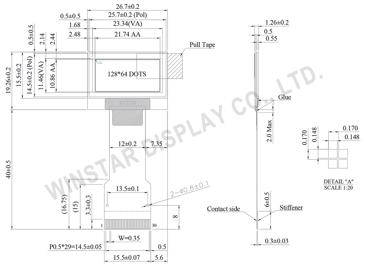
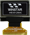
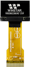
WEO012864C 是一款高性能 0.96 英寸 128x64 COG (Chip on Glass) OLED 显示模块,内置 SH1106 控制 IC。其 0.96 英寸 OLED 模块尺寸仅为 26.70 x 19.26 mm,专为空间受限的物联网终端、穿戴设备及工业仪表设计,兼具高可靠性与通用性。
凭借坚固的 COG 封装与灵活的硬件配置,WEO012864C 0.96 英寸 OLED 模块 助力研发团队针对特定专业应用选择最优硬件方案。
 可选 FPC
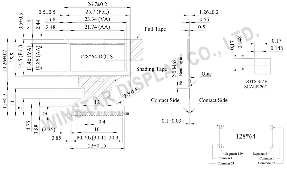
| 项目 | 规格 | 单位 |
|---|---|---|
| 点阵(分辨率) | 128 x 64 | - |
| 模块尺寸 | 26.70 × 19.26 ×1.26 | mm |
| 有效区域 | 21.74 × 10.86 | mm |
| 点大小 | 0.148 × 0.148 | mm |
| 点间距 | 0.170 × 0.170 | mm |
| 显示模式 | 被动矩阵 | |
| 发光颜色 | 单色 | |
| 驱动方式 | 1/64 Duty | |
| 控制器IC | SH1106 | |
| 接口 | 6800, 8080, SPI, I2C | |
| 尺寸 | 0.96 寸 | |
| 参数 | 符号 | 最小值 | 最大值 | 单位 |
|---|---|---|---|---|
| 逻辑电源电压 | VDD1 | -0.3 | 3.6 | V |
| 电荷帮浦电源 | VDD2 | -0.3 | 4.8 | V |
| 显示电源电压 | VPP | -0.3 | 14.5 | V |
| 工作温度 | TOP | -40 | +80 | °C |
| 储存温度 | TSTG | -40 | +85 | °C |
| 项目 | 符号 | 条件 | 最小值 | 典型值 | 最大值 | 单位 |
|---|---|---|---|---|---|---|
| 逻辑电源电压 | VDD1 | - | 2.8 | 3.0 | 3.3 | V |
| 电荷帮浦电源 | VDD2 | - | 3.5 | 3.8 | 4.2 | V |
| 显示器的电荷帮浦输出电压 (Generated by Internal DC/DC) |
Charge Pump VPP |
- | 7.5 | 8 | 8.5 | V |
| 输入高准位 | VIH | - | 0.8xVDD1 | - | VDD1 | V |
| 输入低准位 | VIL | - | VSS | - | 0.2xVDD1 | V |
| 输出高准位 | VOH | - | 0.8xVDD1 | - | VDD1 | V |
| 输出低准位 | VOL | - | VSS | - | 0.2xVDD1 | V |
| VDD2的工作电流显示50%ON | IDD2 | - | - | 10 | 16 | mA |
| No. | 符号 | 功能说明 | |||||||||||||||
|---|---|---|---|---|---|---|---|---|---|---|---|---|---|---|---|---|---|
| 1 | NC | No connection | |||||||||||||||
| 2 | C1N | Connect to charge pump capacitor. These pins are not used and should be disconnected when Vpp is supplied externally. |
|||||||||||||||
| 3 | C1P | ||||||||||||||||
| 4 | C2P | Connect to charge pump capacitor. These pins are not used and should be disconnected when Vpp is supplied externally. |
|||||||||||||||
| 5 | C2N | ||||||||||||||||
| 6 | VDD2 | 3.0 – 4.7V power supply pad for Power supply for charge pump circuit. This pin should be disconnected when VPP is supplied externally |
|||||||||||||||
| 7 | NC | No connection | |||||||||||||||
| 8 | VSS | Ground. | |||||||||||||||
| 9 | VDD1 | Power supply input: 1.65 - 3.5V | |||||||||||||||
| 10 | NC | No connection | |||||||||||||||
| 11 | IM1 | These are the MPU interface mode select pads.
|
|||||||||||||||
| 12 | IM2 | ||||||||||||||||
| 13 | CSB | This pad is the chip select input. When CSB = “L”, then the chip select becomes active, and data/command I/O is enabled. | |||||||||||||||
| 14 | RESB | This is a reset signal input pad. When RES is set to “L”, the settings are initialized. The reset operation is performed by the RES signal level. | |||||||||||||||
| 15 | A0 | This is the Data/Command control pad that determines whether the data bits are data or a command. A0 = “H”: the inputs at D0 to D7 are treated as display data. A0 = “L”: the inputs at D0 to D7 are transferred to the command registers. In I2C interface, this pad serves as SA0 to distinguish the different address of OLED driver. |
|||||||||||||||
| 16 | WRB | This is a MPU interface input pad. When connected to an 8080 MPU, this is active LOW. This pad connects to the 8080 MPU WR signal. The signals on the data bus are latched at the rising edge of the WR signal. When connected to a 6800 Series MPU: This is the read/write control signal input terminal. When R/W = “H”: Read. When R/W = “L”: Write. |
|||||||||||||||
| 17 | RDB | This is a MPU interface input pad. When connected to an 8080 series MPU, it is active LOW. This pad is connected to the RD signal of the 8080 series MPU, and the data bus is in an output status when this signal is “L”. When connected to a 6800 series MPU , this is active HIGH. This is used as an enable clock input of the 6800 series MPU. When RD = “H”: Enable. When RD = “L”: Disable. |
|||||||||||||||
| 18 | D0 | This is an 8-bit bi-directional data bus that connects to an 8-bit or 16-bit standard MPU data bus. When the serial interface is selected, then D0 serves as the serial clock input pad (SCL) and D1 serves as the serial data input pad (SI). At this time, D2 to D7 are set to high impedance. When the I2C interface is selected, then D0 serves as the serial clock input pad (SCL) and D1 serves as the serial data input pad (SDAI). At this time, D2 to D7 are set to high impedance. |
|||||||||||||||
| 19 | D1 | ||||||||||||||||
| 20 | D2 | ||||||||||||||||
| 21 | D3 | ||||||||||||||||
| 22 | D4 | ||||||||||||||||
| 23 | D5 | ||||||||||||||||
| 24 | D6 | ||||||||||||||||
| 25 | D7 | ||||||||||||||||
| 26 | IREF | This is a segment current reference pad. A resistor should be connected between this pad and VSS. Set the current at 18.75uA. | |||||||||||||||
| 27 | VCOMH | This is a pad for the voltage output high level for common signals. A capacitor should be connected between this pad and VSS. |
|||||||||||||||
| 28 | VPP | OLED panel power supply. Generated by internal charge pump. Connect to capacitor. It could be supplied externally. |
|||||||||||||||
| 29 | NC | No connection | |||||||||||||||
| 30 | NC | No connection |
| Drawing | FPC Length | PIN | Pitch | ZIF FPC or HOTBAR FPC | Interface | FPC No. | Create Date |
|---|---|---|---|---|---|---|---|
 |
13 | 30 | 0.7 | HOTBAR FPC | 6800, 8080, 4-Wire SPI, I2C | FPC2070003001XXXXX09 | 20180613 |
 |
40.95 | 30 | 0.5 | ZIF | 6800, 8080, SPI, I2C | FPC2050003011XXXXX23 | 20190412 |

通过点击「允许所有 Cookie」,代表您同意在您的设备上存储 Cookie 以增强网站浏览体验、分析网站使用情况并协助我们的营销和网站效能优化工作。您可以在我们的隐私权政策中找到有关于此的更多信息。