我们重视您的隐私
通过点击「允许所有 Cookie」,代表您同意在您的设备上存储 Cookie 以增强网站浏览体验、分析网站使用情况并协助我们的营销和网站效能优化工作。您可以在我们的隐私权政策中找到有关于此的更多信息。


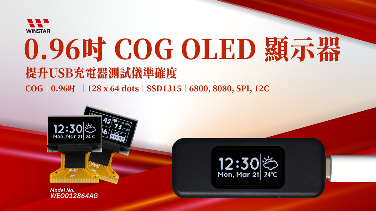
WEO012864AG 是一款单色被动式矩阵 OLED 显示模块,采用绘图型 COG(Chip-on-Glass)结构,对角线尺寸为 0.96寸,具有 128x64 dots的分辨率和高的对比度为 10,000:1。其逻辑供电电压为 3V,驱动方式为 1/64 Duty。WEO012864AG 系列 单色 OLED 内置 SSD1315 IC,支援 8-bit 6800/8080、I2C 和 3 线/4 线 SPI 接口,并提供内部电源升压和外部电源供应选择。
模块工作温度范围 -30℃ ~ +70℃ 之间可靠运行,储存温度范围 -30℃ ~ +70℃。此OLED 模块设计灵活多用,非常适用于医疗设备,如血氧机,以及各种测量仪器,包括USB电源检测器、数字角度尺/角度仪等等。
| 项目 | 标准尺寸 | 单位 |
|---|---|---|
| 点阵(分辨率) | 128 x 64 | - |
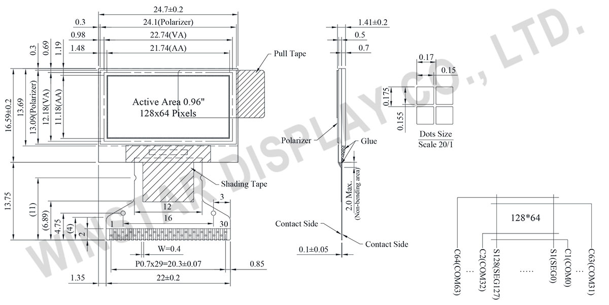
| 模块尺寸 | 24.7 x 16.59 x 1.41 | mm |
| 有效区域 | 21.74 x 11.18 | mm |
| 点大小 | 0.15 x 0.155 | mm |
| 点间距 | 0.17 x 0.175 | mm |
| 显示模式 | 被动矩阵 | |
| 发光颜色 | 单色 | |
| 驱动方式 | 1/64 Duty | |
| IC | SSD1315 | |
| 接口 | 6800,8080,SPI,I2C | |
| 显示尺寸(对角线) | 0.96 寸 | |
| 参数 | 符号 | 最小值 | 最大值 | 单位 |
|---|---|---|---|---|
| 逻辑电源电压 | VDD | 0 | 4 | V |
| 电荷帮浦稳压器电源电压 | VBAT | -0.3 | 6.0 | V |
| 显示电源电压 | VCC | 0 | 18.0 | V |
| 工作温度 | TOP | -30 | +70 | ℃ |
| 储存温度 | TSTG | -30 | +70 | ℃ |
| 项目 | 符号 | 条件 | 最小值 | 典型值 | 最大值 | 单位 |
|---|---|---|---|---|---|---|
| 逻辑电源电压 | VDD | - | 1.65 | 3.0 | 3.3 | V |
| 显示电源电压(外部提供) | VCC | - | 7.5 | - | 8.0 | V |
| 电荷帮浦稳压器电源电压 | VBAT | - | 3.0 | 3.5 | 4.5 | V |
| 显示器的电荷帮浦输出电压 (Generated by Internal DC/DC) | Charge Pump VCC | - | 7.0 | 7.5 | - | V |
| 输入高电压 | VIH | - | 0.8xVDD | - | - | V |
| 输入低电压 | VIL | - | - | - | 0.2VDD | V |
| 输出高电压 | VOH | - | 0.9xVDD | - | - | V |
| 输出低电压 | VOL | - | - | - | 0.1xVDD | V |
| VCC工作电流 (Display 50% Pixel on)(VCC由外部提供) |
ICC | VCC=7.5V | - | 5.0 | 10 | mA |
| Display 50% Pixel on (VCC Generated by Internal DC/DC) |
IBAT | VBAT=3.5V | - | 15 | 22.5 | mA |
| Pin No. | 符号 | 功能 | ||||||||||||||||||||||||
|---|---|---|---|---|---|---|---|---|---|---|---|---|---|---|---|---|---|---|---|---|---|---|---|---|---|---|
| 1 | N.C. (GND) | The supporting pins can reduce the influences from stresses on the function pins. These pins must be connected to external ground. | ||||||||||||||||||||||||
| 2 | C2P | C1P/C1N – Pin for charge pump capacitor; Connect to each other with a capacitor. C2P/C2N – Pin for charge pump capacitor; Connect to each other with a capacitor. |
||||||||||||||||||||||||
| 3 | C2N | |||||||||||||||||||||||||
| 4 | C1P | |||||||||||||||||||||||||
| 5 | C1N | |||||||||||||||||||||||||
| 6 | VBAT | This is the power supply pin for the internal buffer of the DC/DC voltage converter. It must be connected to external source when the converter is used. It should be connected to VDD when the converter is not used. | ||||||||||||||||||||||||
| 7 | NC | NC | ||||||||||||||||||||||||
| 8 | VSS | This is a ground pin. | ||||||||||||||||||||||||
| 9 | VDD | Power supply pin for core logic operation. | ||||||||||||||||||||||||
| 10 | BS0 | These pins are MCU interface selection input. See the following table:
|
||||||||||||||||||||||||
| 11 | BS1 | |||||||||||||||||||||||||
| 12 | BS2 | |||||||||||||||||||||||||
| 13 | CS# | This pin is the chip select input connecting to the MCU. The chip is enabled for MCU communication only when CS# is pulled LOW (active LOW). |
||||||||||||||||||||||||
| 14 | RES# | This pin is reset signal input. When the pin is low, initialization of the chip is executed. Keep this pin HIGH (i.e. connect to VDD) during normal operation. | ||||||||||||||||||||||||
| 15 | D/C# | This pin is Data/Command control pin connecting to the MCU. When the pin is pulled HIGH, the data at D[7:0] will be interpreted as data. When the pin is pulled LOW, the data at D[7:0] will be transferred to a command register. In I2C mode, this pin acts as SA0 for slave address selection. When 3-wire serial interface is selected, this pin must be connected to VSS. |
||||||||||||||||||||||||
| 16 | R/W# | This is read / write control input pin connecting to the MCU interface. When interfacing to a 6800-series microprocessor, this pin will be used as Read/Write (R/W#) selection input. Read mode will be carried out when this pin is pulled HIGH (i.e. connect to VDD) and write mode when LOW. When 8080 interface mode is selected, this pin will be the Write (WR#) input. Data write operation is initiated when this pin is pulled LOW and the chip is selected. When serial or I2C interface is selected, this pin must be connected to VSS. |
||||||||||||||||||||||||
| 17 | E/RD# | This pin is MCU interface input. When 6800 interface mode is selected, this pin will be used as the Enable (E) signal. Read/write operation is initiated when this pin is pulled HIGH and the chip is selected. When 8080 interface mode is selected, this pin receives the Read (RD#) signal. Read operation is initiated when this pin is pulled LOW and the chip is selected. When serial or I2C interface is selected, this pin must be connected to VSS. |
||||||||||||||||||||||||
| 18~25 | D0~D7 | These pins are bi-directional data bus connecting to the MCU data bus. Unused pins are recommended to tie LOW. When serial interface mode is selected, D2 should be either tied LOW or tied together with D1 as the serial data input: SDIN, and D0 will be the serial clock input: SCLK. When I2C mode is selected, D2, D1 should be tied together and serve as SDAout, SDAin in application and D0 is the serial clock input, SCL. |
||||||||||||||||||||||||
| 26 | IREF | When external IREF is used, a resistor should be connected between this pin and VSS to maintain the IREF current at a maximum of 30uA. When internal IREF is used, this pin should be kept NC. |
||||||||||||||||||||||||
| 27 | VCOMH | COM signal deselected voltage level. A capacitor should be connected between this pin and VSS. |
||||||||||||||||||||||||
| 28 | VCC | Power supply for panel driving voltage. This is also the most positive power voltage supply pin. When charge pump is enabled, a capacitor should be connected between this pin and VSS. |
||||||||||||||||||||||||
| 29 | VLSS | This is an analog ground pin. It should be connected to VSS externally. | ||||||||||||||||||||||||
| 30 | NC (GND) |
The supporting pins can reduce the influences from stresses on the function pins. These pins must be connected to external ground. |

通过点击「允许所有 Cookie」,代表您同意在您的设备上存储 Cookie 以增强网站浏览体验、分析网站使用情况并协助我们的营销和网站效能优化工作。您可以在我们的隐私权政策中找到有关于此的更多信息。