
우리는 귀하의 프라이버시를 소중히 여깁니다
"모든 쿠키 허용"을 클릭하면 사이트 탐색을 개선하고, 사이트 사용을 분석하며, 마케팅 및 성능 노력에 도움을 주기 위해 쿠키를 귀하의 장치에 저장하는 데 동의한 것으로 간주됩니다. 이 주제에 대한 추가 정보는 당사의 정책에서 확인할 수 있습니다. 개인정보 보호정책


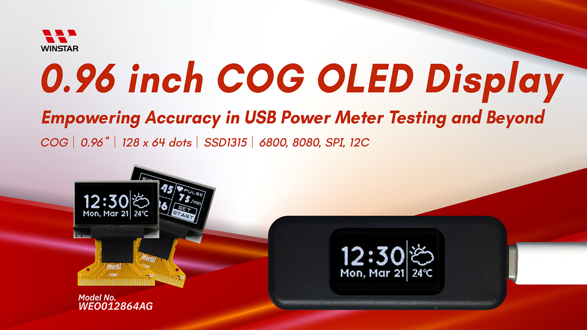
WEO012864AG는 그래픽 COG (Chip-on-Glass) 구조를 갖춘 0.96인치 대각선 크기의 단색 패시브 매트릭스 OLED 디스플레이 모듈입니다. 해상도는 128x64 도트이며, 대비 비율은 10000:1로 높습니다. 3V 로직 전원 공급으로 작동하며, 듀티 사이클은 1/64입니다. 이 WEO012864AG 시리즈의 단색 OLED는 SSD1315 IC를 장착하여 8비트 6800/8080, I2C 및 3선/4선 SPI 인터페이스를 지원하며 내부 전원 부스트 및 외부 전원 공급 옵션을 제공합니다.
이 OLED 모듈은 -30℃에서 +70℃의 온도 범위 내에서 안정적으로 작동하며, 저장 온도는 -30℃에서 +70℃입니다. 이 OLED 모듈은 산소 측정기와 같은 의료 장비뿐만 아니라 USB 전원 감지기, 디지털 각도 자/각도 측정기 등 다양한 측정 기기에서 탁월한 유연성을 발휘합니다.
| 항목 | 치수 | 단위 |
|---|---|---|
| 표시 형식 | 128 x 64 | - |
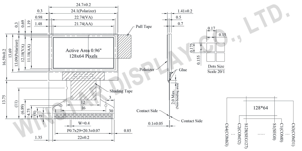
| 모듈 치수 | 24.7 x 16.59 x 1.41 | mm |
| 활성 영역 | 21.74 x 11.18 | mm |
| 도트 크기 | 0.15 x 0.155 | mm |
| 도트 피치 | 0.17 x 0.175 | mm |
| 디스플레이 모드 | 패시브 매트릭스 | |
| 디스플레이 색상 | Monochrome | |
| 듀티 | 1/64 Duty | |
| IC | SSD1315 | |
| 인터페이스 | 6800,8080,SPI,I2C | |
| 크기 (대각선) | 0.96 인치 | |
| Parameter | 기호 | 최소값 | 최대값 | 단위 |
|---|---|---|---|---|
| Supply Voltage For Logic | VDD | 0 | 4 | V |
| Charge Pump Regulator Supply Voltage | VBAT | -0.3 | 6.0 | V |
| Supply Voltage for Display | VCC | 0 | 18.0 | V |
| 작동 온도 | TOP | -30 | +70 | ℃ |
| 보관 온도 | TSTG | -30 | +70 | ℃ |
| 항목 | 기호 | 조건 | 최소값 | 대표값 | 최대값 | 단위 |
|---|---|---|---|---|---|---|
| Supply Voltage For Logic | VDD | - | 1.65 | 3.0 | 3.3 | V |
| Supply Voltage for Display(Supplied Externally) | VCC | - | 7.5 | - | 8.0 | V |
| Charge Pump Regulator Supply Voltage | VBAT | - | 3.0 | 3.5 | 4.5 | V |
| Charge Pump Output Voltage for Display (Generated by Internal DC/DC) | Charge Pump VCC | - | 7.0 | 7.5 | - | V |
| Input High Volt. | VIH | - | 0.8xVDD | - | - | V |
| Input Low Volt. | VIL | - | - | - | 0.2VDD | V |
| Output High Volt. | VOH | - | 0.9xVDD | - | - | V |
| Output Low Volt. | VOL | - | - | - | 0.1xVDD | V |
| Operating Current for VCC (Display 50% Pixel on)(VCC Supplied Externally) |
ICC | VCC=7.5V | - | 5.0 | 10 | mA |
| Display 50% Pixel on (VCC Generated by Internal DC/DC) |
IBAT | VBAT=3.5V | - | 15 | 22.5 | mA |
| Pin No. | 기호 | 기능 | ||||||||||||||||||||||||
|---|---|---|---|---|---|---|---|---|---|---|---|---|---|---|---|---|---|---|---|---|---|---|---|---|---|---|
| 1 | N.C. (GND) | The supporting pins can reduce the influences from stresses on the function pins. These pins must be connected to external ground. | ||||||||||||||||||||||||
| 2 | C2P | C1P/C1N – Pin for charge pump capacitor; Connect to each other with a capacitor. C2P/C2N – Pin for charge pump capacitor; Connect to each other with a capacitor. |
||||||||||||||||||||||||
| 3 | C2N | |||||||||||||||||||||||||
| 4 | C1P | |||||||||||||||||||||||||
| 5 | C1N | |||||||||||||||||||||||||
| 6 | VBAT | This is the power supply pin for the internal buffer of the DC/DC voltage converter. It must be connected to external source when the converter is used. It should be connected to VDD when the converter is not used. | ||||||||||||||||||||||||
| 7 | NC | NC | ||||||||||||||||||||||||
| 8 | VSS | This is a ground pin. | ||||||||||||||||||||||||
| 9 | VDD | Power supply pin for core logic operation. | ||||||||||||||||||||||||
| 10 | BS0 | These pins are MCU interface selection input. See the following table:
|
||||||||||||||||||||||||
| 11 | BS1 | |||||||||||||||||||||||||
| 12 | BS2 | |||||||||||||||||||||||||
| 13 | CS# | This pin is the chip select input connecting to the MCU. The chip is enabled for MCU communication only when CS# is pulled LOW (active LOW). |
||||||||||||||||||||||||
| 14 | RES# | This pin is reset signal input. When the pin is low, initialization of the chip is executed. Keep this pin HIGH (i.e. connect to VDD) during normal operation. | ||||||||||||||||||||||||
| 15 | D/C# | This pin is Data/Command control pin connecting to the MCU. When the pin is pulled HIGH, the data at D[7:0] will be interpreted as data. When the pin is pulled LOW, the data at D[7:0] will be transferred to a command register. In I2C mode, this pin acts as SA0 for slave address selection. When 3-wire serial interface is selected, this pin must be connected to VSS. |
||||||||||||||||||||||||
| 16 | R/W# | This is read / write control input pin connecting to the MCU interface. When interfacing to a 6800-series microprocessor, this pin will be used as Read/Write (R/W#) selection input. Read mode will be carried out when this pin is pulled HIGH (i.e. connect to VDD) and write mode when LOW. When 8080 interface mode is selected, this pin will be the Write (WR#) input. Data write operation is initiated when this pin is pulled LOW and the chip is selected. When serial or I2C interface is selected, this pin must be connected to VSS. |
||||||||||||||||||||||||
| 17 | E/RD# | This pin is MCU interface input. When 6800 interface mode is selected, this pin will be used as the Enable (E) signal. Read/write operation is initiated when this pin is pulled HIGH and the chip is selected. When 8080 interface mode is selected, this pin receives the Read (RD#) signal. Read operation is initiated when this pin is pulled LOW and the chip is selected. When serial or I2C interface is selected, this pin must be connected to VSS. |
||||||||||||||||||||||||
| 18~25 | D0~D7 | These pins are bi-directional data bus connecting to the MCU data bus. Unused pins are recommended to tie LOW. When serial interface mode is selected, D2 should be either tied LOW or tied together with D1 as the serial data input: SDIN, and D0 will be the serial clock input: SCLK. When I2C mode is selected, D2, D1 should be tied together and serve as SDAout, SDAin in application and D0 is the serial clock input, SCL. |
||||||||||||||||||||||||
| 26 | IREF | When external IREF is used, a resistor should be connected between this pin and VSS to maintain the IREF current at a maximum of 30uA. When internal IREF is used, this pin should be kept NC. |
||||||||||||||||||||||||
| 27 | VCOMH | COM signal deselected voltage level. A capacitor should be connected between this pin and VSS. |
||||||||||||||||||||||||
| 28 | VCC | Power supply for panel driving voltage. This is also the most positive power voltage supply pin. When charge pump is enabled, a capacitor should be connected between this pin and VSS. |
||||||||||||||||||||||||
| 29 | VLSS | This is an analog ground pin. It should be connected to VSS externally. | ||||||||||||||||||||||||
| 30 | NC (GND) |
The supporting pins can reduce the influences from stresses on the function pins. These pins must be connected to external ground. |

"모든 쿠키 허용"을 클릭하면 사이트 탐색을 개선하고, 사이트 사용을 분석하며, 마케팅 및 성능 노력에 도움을 주기 위해 쿠키를 귀하의 장치에 저장하는 데 동의한 것으로 간주됩니다. 이 주제에 대한 추가 정보는 당사의 정책에서 확인할 수 있습니다. 개인정보 보호정책