

 - WEO012864AH")
우리는 귀하의 프라이버시를 소중히 여깁니다
"모든 쿠키 허용"을 클릭하면 사이트 탐색을 개선하고, 사이트 사용을 분석하며, 마케팅 및 성능 노력에 도움을 주기 위해 쿠키를 귀하의 장치에 저장하는 데 동의한 것으로 간주됩니다. 이 주제에 대한 추가 정보는 당사의 정책에서 확인할 수 있습니다. 개인정보 보호정책

 - WEO012864D")
 - WEO012864D")
 - WEO012864D")
 - WEO012864D")
 - WEO012864D")
 - WEO012864D")
 - WEO012864D")
 - WEO012864D")
 - WEO012864D")
 - WEO012864D")
 - WEO012864D")
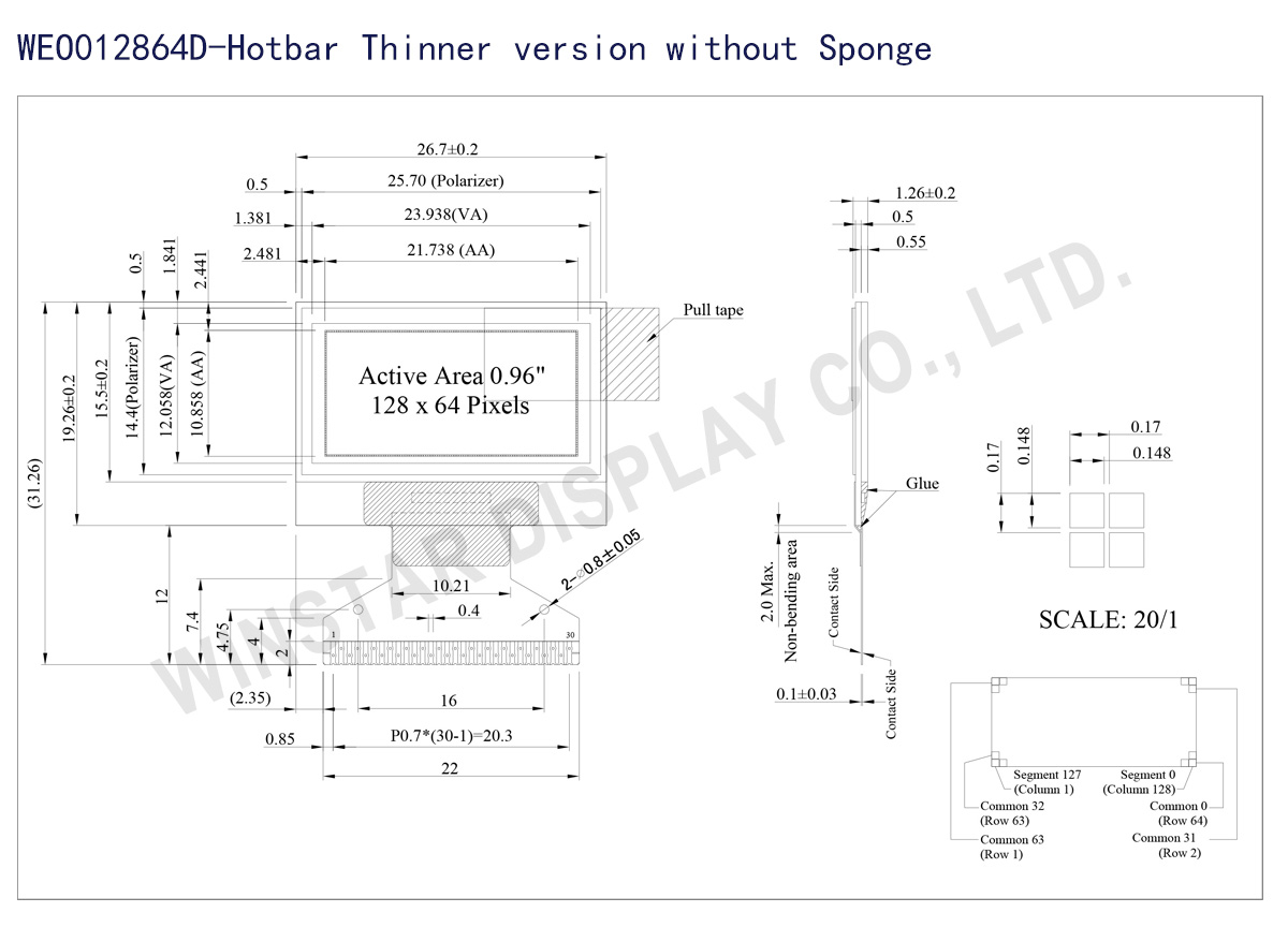
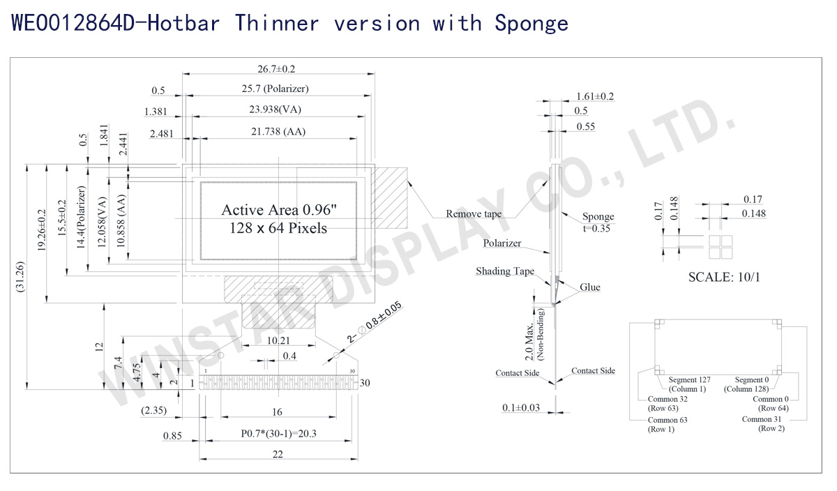
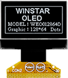
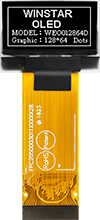
WEO012864D는 Winstar의 주력 0.96인치 COG 타입 OLED 디스플레이 모듈입니다. 128x64 해상도와 SSD1306 IC를 탑재하였으며, 이미 시장에서 검증된 신뢰성과 높은 호환성을 바탕으로 각종 산업용 기기 및 소비자 가전에 폭넓게 채택되고 있습니다.
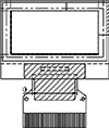
WEO012864D 시리즈는 두 가지 두께 프로파일로 제공됩니다. 두 버전 모두 전기적 특성과 핀 맵(Pin Assignment)은 동일합니다.

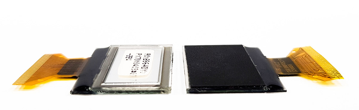
왼쪽: 표준 슬림 버전 (1.26mm) | 오른쪽: 스펀지 부착 버전 (1.61mm 호환용)
| 항목 | WEO012864D-Hotbar | WEO012864D-Hotbar with Sponge | 단위 |
|---|---|---|---|
| 도트 매트릭스 | 128 × 64 | 점 | |
| 모듈 치수 | 26.7 × 19.26 × 1.26 | 26.7 × 19.26 × 1.61 | mm |
| 활성 영역 | 21.738 × 10.858 | mm | |
| 도트 크기 | 0.148 × 0.148 | mm | |
| 도트 피치 | 0.17 × 0.17 | mm | |
| 디스플레이 모드 | 패시브 매트릭스 | ||
| 디스플레이 색상 | Monochrome | ||
| Drive Duty | 1/64 Duty | ||
| IC | SSD1306 | ||
| 인터페이스 | 6800,8080,SPI,I2C | ||
| 크기 | 0.96 인치 | ||
| Parameter | 기호 | 최소값 | 최대값 | 단위 |
|---|---|---|---|---|
| Supply Voltage for Logic | VDD | 0 | 4.0 | V |
| Supply Voltage for Display | VCC | 0 | 15.0 | V |
| 작동 온도 | TOP | -40 | +80 | °C |
| 보관 온도 | TSTG | -40 | +85 | °C |
| 항목 | 기호 | 조건 | 최소값 | 대표값 | 최대값 | 단위 |
|---|---|---|---|---|---|---|
| Supply Voltage for Logic | VDD | - | 2.8 | 3.0 | 3.3 | V |
| Supply Voltage for Display | VCC | - | 11.5 | 12.0 | 12.5 | V |
| Input High Volt. | VIH | - | 0.8×VDD | - | VDDIO | V |
| Input Low Volt. | VIL | - | 0 | - | 0.2×VDD | V |
| Output High Volt. | VOH | - | 0.9×VDD | - | VDDIO | V |
| Output Low Volt. | VOL | - | 0 | - | 0.1×VDD | V |
| Operating Current for VCC (50% display ON) | ICC | - | - | 16.0 | 20.0 | mA |
| No. | 기호 | 기능 |
|---|---|---|
| 1 | N.C. (GND) | Reserved Pin (Supporting Pin) The supporting pins can reduce the influences from stresses on the function pins. These pins must be connected to external ground. |
| 2 | C2N | Positive Terminal of the Flying Inverting Capacitor Negative Terminal of the Flying Boost Capacitor The charge-pump capacitors are required between the terminals. They must be floated when the converter is not used. |
| 3 | C2P | |
| 4 | C1P | |
| 5 | C1N | |
| 6 | VBAT | Power Supply for DC/DC Converter Circuit This is the power supply pin for the internal buffer of the DC/DC voltage converter. It must be connected to external source when the converter is used. It should be connected to VDD when the converter is not used. |
| 7 | NC | NC |
| 8 | VSS | Ground of Logic Circuit This is a ground pin. It acts as a reference for the logic pins. It must be connected to external ground. |
| 9 | VDD | Power Supply for Logic This is a voltage supply pin. It must be connected to external source. |
| 10 | BS0 | Communicating Protocol Select These pins are MCU interface selection input. See the following table: 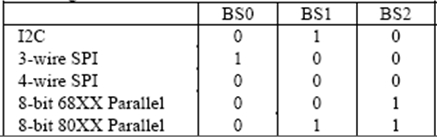 |
| 11 | BS1 | |
| 12 | BS2 | |
| 13 | CS# | Chip Select This pin is the chip select input. The chip is enabled for MCU communication only when CS# is pulled low. |
| 14 | RES# | Power Reset for Controller and Driver This pin is reset signal input. When the pin is low, initialization of the chip is executed. |
| 15 | D/C# | Data/Command Control This pin is Data/Command control pin. When the pin is pulled high, the input at D7~D0 is treated as display data. When the pin is pulled low, the input at D7~D0 will be transferred to the command register. For detail relationship to MCU interface signals, please refer to the Timing Characteristics Diagrams. When the pin is pulled high and serial interface mode is selected, the data at SDIN is treated as data. When it is pulled low, the data at SDIN will be transferred to the command register. In I2C mode, this pin acts as SA0 for slave address selection. |
| 16 | R/W# | Read/Write Select or Write This pin is MCU interface input. When interfacing to a 68XX-series microprocessor, this pin will be used as Read/Write (R/W#) selection input. Pull this pin to “High” for read mode and pull it to “Low” for write mode. When 80XX interface mode is selected, this pin will be the Write (WR#) input. Data write operation is initiated when this pin is pulled low and the CS# is pulled low. |
| 17 | E/RD# | Read/Write Enable or Read This pin is MCU interface input. When interfacing to a 68XX-series microprocessor, this pin will be used as the Enable (E) signal. Read/write operation is initiated when this pin is pulled high and the CS# is pulled low. When connecting to an 80XX-microprocessor, this pin receives the Read (RD#) signal. Data read operation is initiated when this pin is pulled low and CS# is pulled low. |
| 18~25 | D0~D7 | Host Data Input/Output Bus These pins are 8-bit bi-directional data bus to be connected to the microprocessor’s data bus. When serial mode is selected, D1 will be the serial data input SDIN and D0 will be the serial clock input SCLK. When I2C mode is selected, D2 & D1 should be tired together and serve as SDAout & SDAin in application and D0 is the serial clock input SCL. |
| 26 | IREF | Current Reference for Brightness Adjustment This pin is segment current reference pin. A resistor should be connected between this pin and VSS. Set the current lower than 12.5μA. |
| 27 | VCOMH | Voltage Output High Level for COM Signal This pin is the input pin for the voltage output high level for COM signals. A capacitor should be connected between this pin and VSS. |
| 28 | VCC | Power Supply for OEL Panel This is the most positive voltage supply pin of the chip. A stabilization capacitor should be connected between this pin and VSS when the converter is used. It must be connected to external source when the converter is not used. |
| 29 | VLSS | Ground of Analog Circuit This is an analog ground pin. It should be connected to VSS externally. |
| 30 | NC (GND) |
Reserved Pin (Supporting Pin) The supporting pins can reduce the influences from stresses on the function pins. These pins must be connected to external ground. |
| 그림 | FPC Length | PIN | Pitch | ZIF FPC or HOTBAR FPC | 인터페이스 | FPC No. | Create Date |
|---|---|---|---|---|---|---|---|
 |
22 | 30 | 0.7 | HOTBAR | 6800,8080,SPI,I2C | FPC2070003001XXXXX08 | 20170808 |
 |
41.1 | 30 | 0.5 | ZIF | 6800,8080,SPI,I2C | FPC2050003011XXXXX28 | 20180604 |
 |
13.1 | 30 | 0.5 | ZIF | 6800,8080,SPI,I2C | FPC2050003011XXXXX34 | 20200221 |

"모든 쿠키 허용"을 클릭하면 사이트 탐색을 개선하고, 사이트 사용을 분석하며, 마케팅 및 성능 노력에 도움을 주기 위해 쿠키를 귀하의 장치에 저장하는 데 동의한 것으로 간주됩니다. 이 주제에 대한 추가 정보는 당사의 정책에서 확인할 수 있습니다. 개인정보 보호정책