
私たちはあなたのプライバシーを大切にします
「すべてのクッキーを許可」をクリックすると、サイトのナビゲーションを向上させ、サイト使用状況を分析し、マーケティングおよびパフォーマンスの取り組みを支援するために、クッキーをデバイスに保存することに同意したことになります。この件に関する詳細情報は、ポリシーをご覧ください。プライバシーポリシー

 - WEO012864D")
 - WEO012864D")
 - WEO012864D")
 - WEO012864D")
 - WEO012864D")
 - WEO012864D")
 - WEO012864D")
 - WEO012864D")
 - WEO012864D")
 - WEO012864D")
 - WEO012864D")
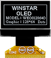
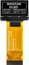
型番 WEO012864D
►薄板バージョン, 有機EL薄型
►タイプ: 有機ELディスプレイ
►結構: COG
►サイズ: 0.96インチ
►128 x 64 ドットマトリックス
►IC:SSD1306
►3V電源電圧
►1/64 duty
►インターフェース: 6800, 8080, SPI, I2C
►発光色: 白色 / 黄色 / 青色
►Other FPC options available in below table
WEO012864Dは、WINSTAR(ウィンスター)を代表する0.96インチCOGタイプの有機EL(OLED)ディスプレイモジュールです。128x64の解像度と、定評のあるSSD1306 ICを内蔵しています。長年の実績がある標準的なモジュールの為、高い信頼性と互換性を備えており、産業機器からコンシューマー製品まで幅広い用途に採用されています。
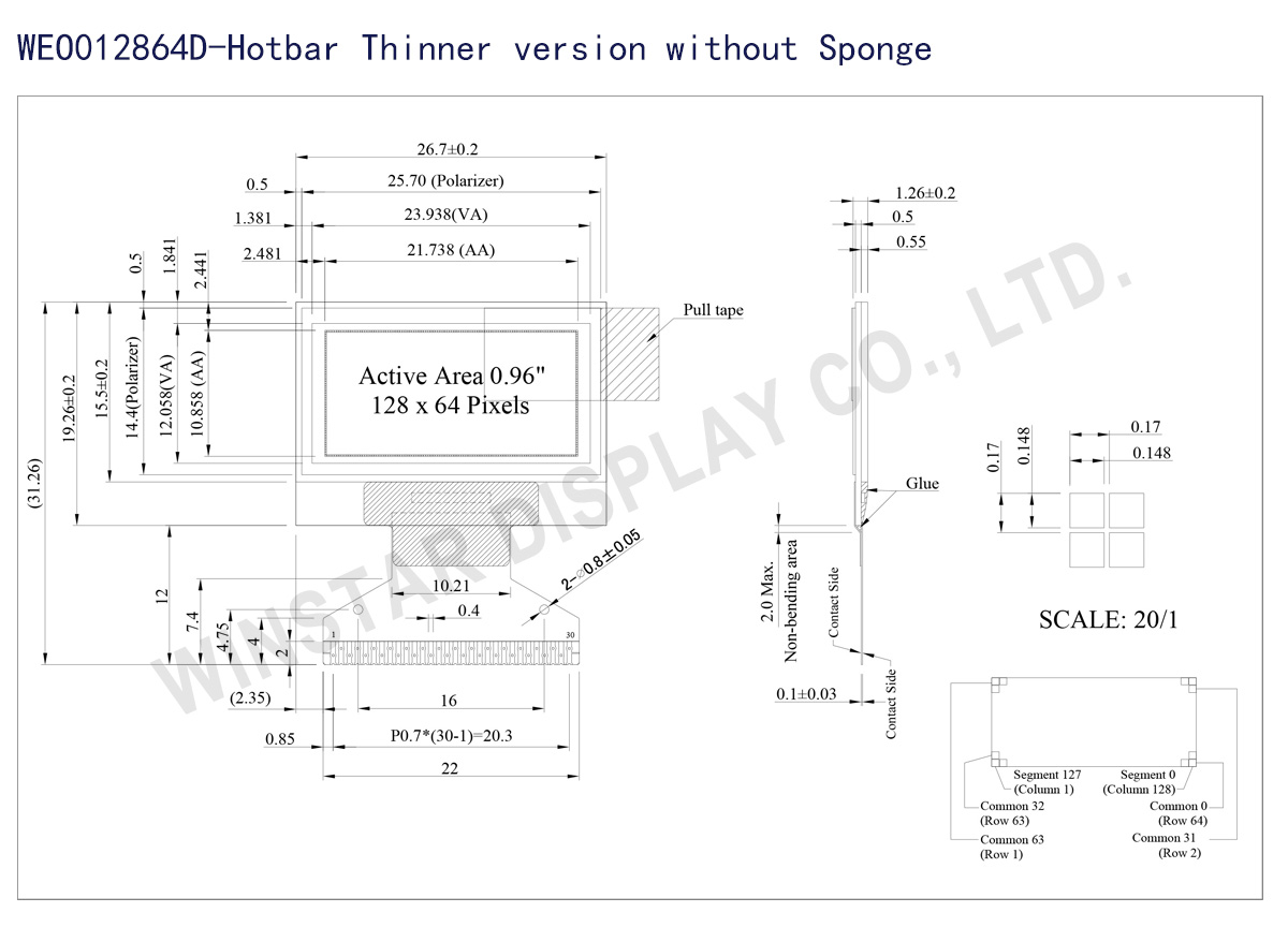
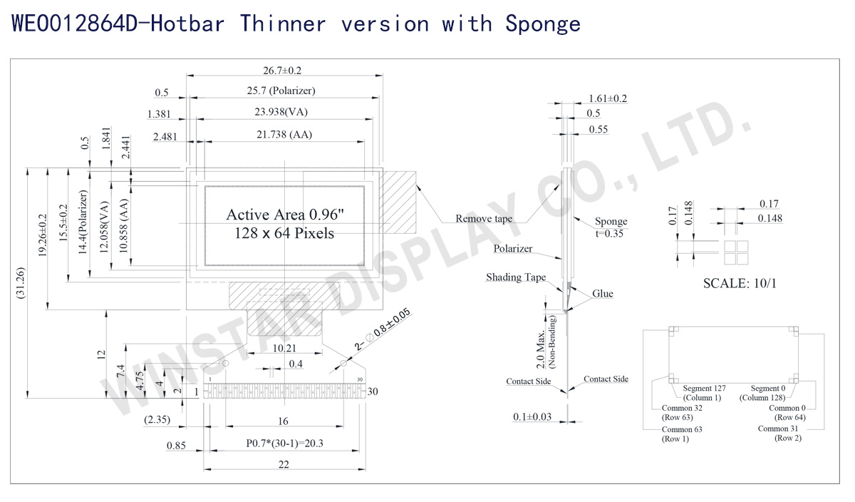
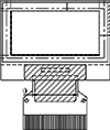
WEO012864Dシリーズは、厚みの異なる2つのプロファイルを用意しています。両バージョンとも電気的特性およびピンアサイン(Pin Assignment)は共通です。

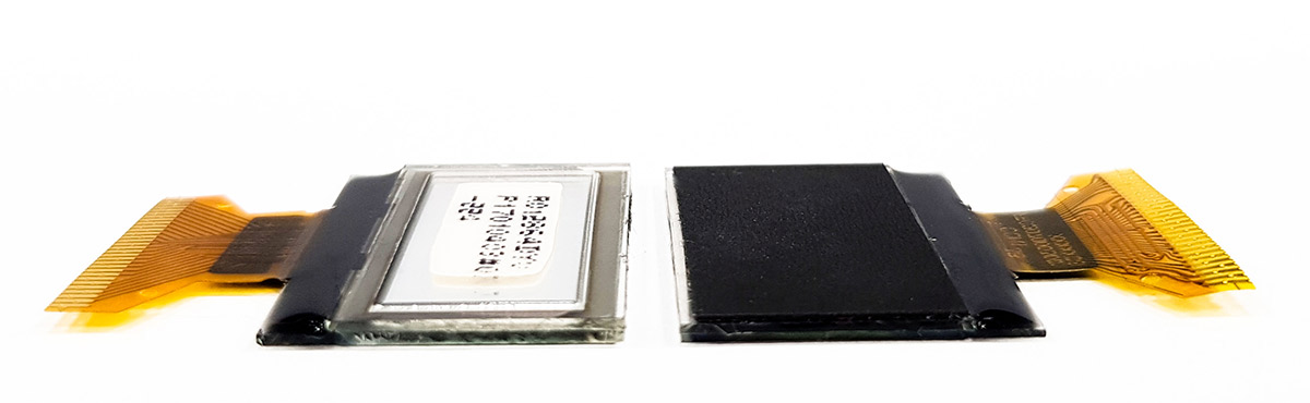
左: 標準スリム版 (1.26mm) | 右: スポンジ付バージョン (1.61mm互換用)
| Item | WEO012864D-Hotbar | WEO012864D-Hotbar スポンジ付き | 単位 |
|---|---|---|---|
| ドットマトリックス | 128 × 64 | Dots | |
| モジュールサイズ | 26.7 × 19.26 × 1.26 | 26.7 × 19.26 × 1.61 | mm |
| アクティブエリア | 21.738 × 10.858 | mm | |
| ドットサイズ | 0.148 × 0.148 | mm | |
| ドットピッチ | 0.17 × 0.17 | mm | |
| 表示モード | パッシブマトリクス | ||
| 発光色 | モノクロ | ||
| 駆動方法 | 1/64 Duty | ||
| IC | SSD1306 | ||
| インターフェイス | 6800,8080,SPI,I2C | ||
| ドットサイズ | 0.96 インチ | ||
| パラメーター | 記号 | 最小値 | 最大値 | 単位 |
|---|---|---|---|---|
| ロジック電源電圧 | VDD | 0 | 4.0 | V |
| Display電源電圧 | VCC | 0 | 15.0 | V |
| 操作温度 | TOP | -40 | +80 | °C |
| 保存温度 | TSTG | -40 | +85 | °C |
| 項目 | 記号 | 条件 | 最小値 | 典型値 | 最大値 | 単位 |
|---|---|---|---|---|---|---|
| ロジック電源電圧 | VDD | - | 2.8 | 3.0 | 3.3 | V |
| Display電源電圧 | VCC | - | 11.5 | 12.0 | 12.5 | V |
| 入力電圧(High) | VIH | - | 0.8×VDD | - | VDDIO | V |
| 入力電圧(Low) | VIL | - | 0 | - | 0.2×VDD | V |
| 出力電圧(High) | VOH | - | 0.9×VDD | - | VDDIO | V |
| 出力電圧(Low) | VOL | - | 0 | - | 0.1×VDD | V |
| Operating Current for VCC (50% display ON) | ICC | - | - | 16.0 | 20.0 | mA |
| No. | 記号 | 説明 |
|---|---|---|
| 1 | N.C. (GND) | Reserved Pin (Supporting Pin) The supporting pins can reduce the influences from stresses on the function pins. These pins must be connected to external ground. |
| 2 | C2N | Positive Terminal of the Flying Inverting Capacitor Negative Terminal of the Flying Boost Capacitor The charge-pump capacitors are required between the terminals. They must be floated when the converter is not used. |
| 3 | C2P | |
| 4 | C1P | |
| 5 | C1N | |
| 6 | VBAT | Power Supply for DC/DC Converter Circuit This is the power supply pin for the internal buffer of the DC/DC voltage converter. It must be connected to external source when the converter is used. It should be connected to VDD when the converter is not used. |
| 7 | NC | NC |
| 8 | VSS | Ground of Logic Circuit This is a ground pin. It acts as a reference for the logic pins. It must be connected to external ground. |
| 9 | VDD | Power Supply for Logic This is a voltage supply pin. It must be connected to external source. |
| 10 | BS0 | Communicating Protocol Select These pins are MCU interface selection input. See the following table: 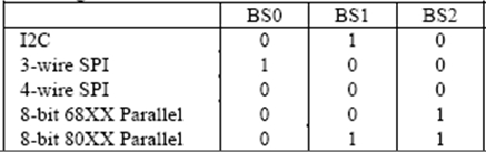 |
| 11 | BS1 | |
| 12 | BS2 | |
| 13 | CS# | Chip Select This pin is the chip select input. The chip is enabled for MCU communication only when CS# is pulled low. |
| 14 | RES# | Power Reset for Controller and Driver This pin is reset signal input. When the pin is low, initialization of the chip is executed. |
| 15 | D/C# | Data/Command Control This pin is Data/Command control pin. When the pin is pulled high, the input at D7~D0 is treated as display data. When the pin is pulled low, the input at D7~D0 will be transferred to the command register. For detail relationship to MCU interface signals, please refer to the Timing Characteristics Diagrams. When the pin is pulled high and serial interface mode is selected, the data at SDIN is treated as data. When it is pulled low, the data at SDIN will be transferred to the command register. In I2C mode, this pin acts as SA0 for slave address selection. |
| 16 | R/W# | Read/Write Select or Write This pin is MCU interface input. When interfacing to a 68XX-series microprocessor, this pin will be used as Read/Write (R/W#) selection input. Pull this pin to “High” for read mode and pull it to “Low” for write mode. When 80XX interface mode is selected, this pin will be the Write (WR#) input. Data write operation is initiated when this pin is pulled low and the CS# is pulled low. |
| 17 | E/RD# | Read/Write Enable or Read This pin is MCU interface input. When interfacing to a 68XX-series microprocessor, this pin will be used as the Enable (E) signal. Read/write operation is initiated when this pin is pulled high and the CS# is pulled low. When connecting to an 80XX-microprocessor, this pin receives the Read (RD#) signal. Data read operation is initiated when this pin is pulled low and CS# is pulled low. |
| 18~25 | D0~D7 | Host Data Input/Output Bus These pins are 8-bit bi-directional data bus to be connected to the microprocessor’s data bus. When serial mode is selected, D1 will be the serial data input SDIN and D0 will be the serial clock input SCLK. When I2C mode is selected, D2 & D1 should be tired together and serve as SDAout & SDAin in application and D0 is the serial clock input SCL. |
| 26 | IREF | Current Reference for Brightness Adjustment This pin is segment current reference pin. A resistor should be connected between this pin and VSS. Set the current lower than 12.5μA. |
| 27 | VCOMH | Voltage Output High Level for COM Signal This pin is the input pin for the voltage output high level for COM signals. A capacitor should be connected between this pin and VSS. |
| 28 | VCC | Power Supply for OEL Panel This is the most positive voltage supply pin of the chip. A stabilization capacitor should be connected between this pin and VSS when the converter is used. It must be connected to external source when the converter is not used. |
| 29 | VLSS | Ground of Analog Circuit This is an analog ground pin. It should be connected to VSS externally. |
| 30 | NC (GND) |
Reserved Pin (Supporting Pin) The supporting pins can reduce the influences from stresses on the function pins. These pins must be connected to external ground. |
| Drawing | FPC Length | PIN | Pitch | ZIF FPC or HOTBAR FPC | Interface | FPC No. | Create Date |
|---|---|---|---|---|---|---|---|
 |
22 | 30 | 0.7 | HOTBAR | 6800,8080,SPI,I2C | FPC2070003001XXXXX08 | 20170808 |
 |
41.1 | 30 | 0.5 | ZIF | 6800,8080,SPI,I2C | FPC2050003011XXXXX28 | 20180604 |
 |
13.1 | 30 | 0.5 | ZIF | 6800,8080,SPI,I2C | FPC2050003011XXXXX34 | 20200221 |

「すべてのクッキーを許可」をクリックすると、サイトのナビゲーションを向上させ、サイト使用状況を分析し、マーケティングおよびパフォーマンスの取り組みを支援するために、クッキーをデバイスに保存することに同意したことになります。この件に関する詳細情報は、ポリシーをご覧ください。プライバシーポリシー