
我们重视您的隐私
通过点击「允许所有 Cookie」,代表您同意在您的设备上存储 Cookie 以增强网站浏览体验、分析网站使用情况并协助我们的营销和网站效能优化工作。您可以在我们的隐私权政策中找到有关于此的更多信息。


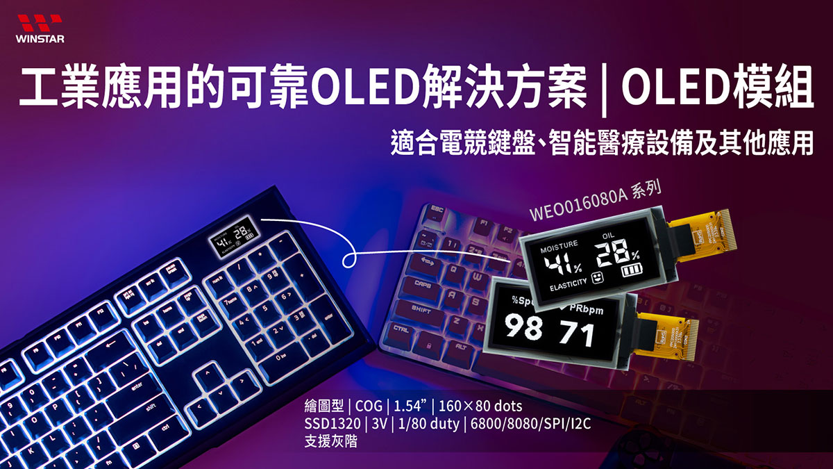
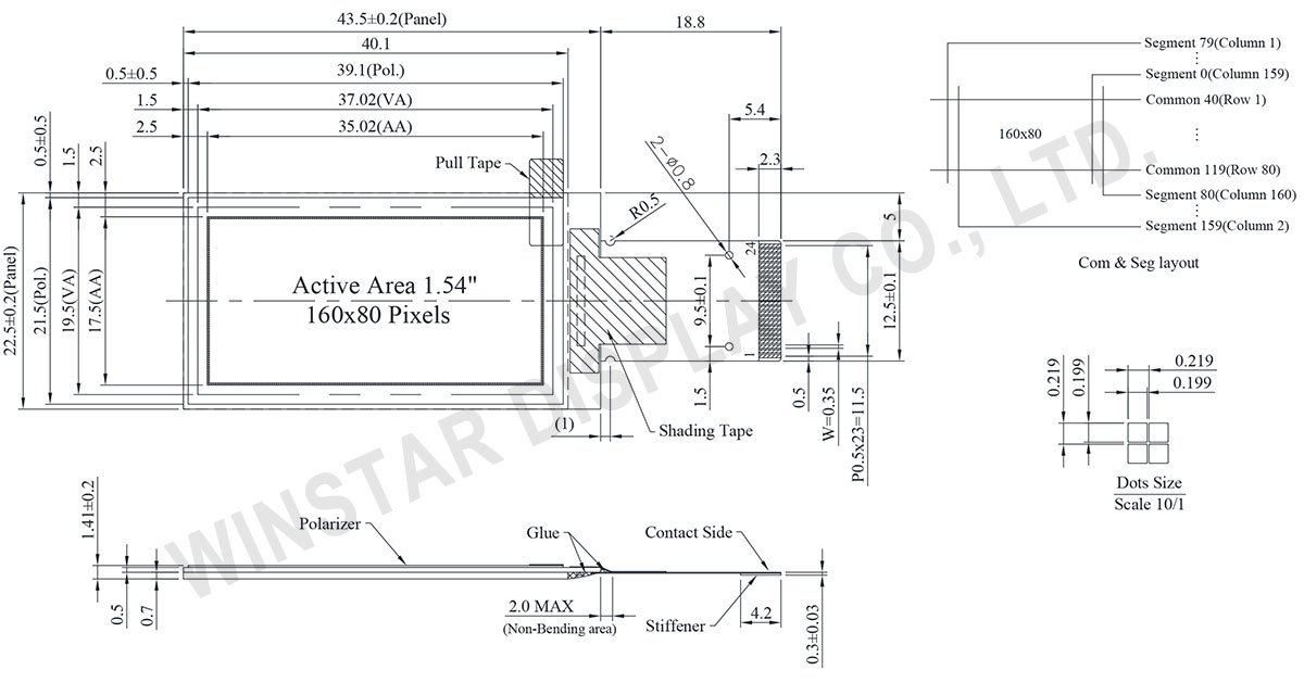
WEO016080A 是一款尺寸为 1.54 寸的 COG 图形 OLED 显示器,分辨率为 160x80 dots。模块尺寸为 43.5 x 22.5 mm,有效显示区域为 35.02 x 17.50 mm,得益于其 COG 结构薄型设计厚度仅 1.41 mm。内置 SSD1320 IC,此模块支持 6800/8080 8-bit、4线 SPI 和 I2C 接口。提供 4-bit (16 Levels) 灰度,并实现高达 10,000:1 的对比度。
支持逻辑电源供应电压范围为 1.65V 至 3.3V (典型值为3V),模块在 -40°C 至 +80°C 的温度范围内可靠运行,并能在 -40°C 至 +85°C 的储存温度下工作。适用于各种应用,包括网络产品、USB 测试仪、智能手表、电竞键盘,以及智能医疗设备如血氧机和皮肤分析仪,WEO016080A 以其清晰生动的显示屏幕提升了显示质量。
高分辨率(160x80 dots) 和低功耗使得这款 OLED 显示模块非常适合要求高性能和高效率的应用。
Data source ref:WEO016080AWPP3N00000
| 项目 | 规格 | 单位 |
|---|---|---|
| 分辨率 | 160 x 80 Dots | - |
| 模块尺寸 | 43.5 x 22.5 x 1.41 | mm |
| 有效区域 | 35.02 x 17.50 | mm |
| 像素大小 | 0.199 x 0.199 | mm |
| 像素间距 | 0.219 x 0.219 | mm |
| 显示模式 | 被动矩阵 | |
| 显示颜色 | 单色 | |
| 驱动方式 | 1/80 Duty | |
| 灰阶 | 4 bits | |
| 接口 | 6800,8080,4-Wire SPI,I2C | |
| IC | SSD1320 | |
| 尺寸 | 1.54 寸 | |
| 参数 | 符号 | 最小值 | 典型值 | 最大值 | 单位 |
|---|---|---|---|---|---|
| 逻辑电源电压 | VDD | -0.3 | - | 4 | V |
| 显示电源电压 | VCC | 0 | - | 19 | V |
| 工作温度 | TOP | -40 | - | +80 | °C |
| 储存温度 | TSTG | -40 | - | +85 | °C |
| 项目 | 符号 | 条件 | 最小值 | 典型值 | 最大值 | 单位 |
|---|---|---|---|---|---|---|
| 逻辑电源电压 | VDD | - | 1.65 | 3.0 | 3.3 | V |
| 逻辑电源电压 | VCC | - | 8.0 | 15.0 | 15.5 | V |
| 输入高电压 | VIH | - | 0.8×VDD | - | VDD | V |
| 输入低电压 | VIL | - | 0 | - | 0.2×VDD | V |
| 输出高电压 | VOH | - | 0.9×VDD | - | VDD | V |
| 输出低电压 | VOL | - | 0 | - | 0.1×VDD | V |
| VCC 供电电流 | ICC | VDD=3V,VCC=15V Display 50% Pixel ON |
- | 14 | 21 | mA |
| No. | 符号 | 功能 | |||||||||||||||
|---|---|---|---|---|---|---|---|---|---|---|---|---|---|---|---|---|---|
| 1 | N.C. (GND) |
Reserved Pin (Supporting Pin) The supporting pin can reduce the influences from stresses on the function pins. This pin could be connected to external ground as the ESD protection circuit. |
|||||||||||||||
| 2 | VCC | Power Supply for OEL Panel This is the most positive voltage supply pin of the chip. It must be connected to external source. |
|||||||||||||||
| 3~4 | N.C. | Reserved Pin The N.C. pin between function pins are reserved for compatible and flexible design. |
|||||||||||||||
| 5 | BS1 | Communicating Protocol Select These pins are MCU interface selection input. See the following table:
|
|||||||||||||||
| 6 | BS2 | ||||||||||||||||
| 7 | VSS | Ground of Logic Circuit This is a ground pin. It also acts as a reference for the logic pins. It must be connected to external ground. |
|||||||||||||||
| 8 | IREF | Current Reference for Brightness Adjustment This pin is segment current reference pin. A resistor should be connected between this pin and VSS. Set the current at 10μA maximum. |
|||||||||||||||
| 9 | CS# | Chip Select This pin is the chip select input. The chip is enabled for MCU communication only when CS# is pulled low. |
|||||||||||||||
| 10 | RES# | Power Reset for Controller and Driver This pin is reset signal input. When the pin is low, initialization of the chip is executed. Keep this pin pull high during normal operation. |
|||||||||||||||
| 11 | D/C# | Data/Command Control This pin is Data/Command control pin. When the pin is pulled high, the input at D7~D0 is treated as display data. When the pin is pulled low, the input at D7~D0 will be transferred to the command register. In I2C mode, this pin acts as SA0 for slave address selection. |
|||||||||||||||
| 12 | R/W# | Read/Write Select or Write This pin is MCU interface input. When interfacing to a 68XX-series microprocessor, this pin will be used as Read/Write (R/W#) selection input. Pull this pin to “High” for read mode and pull it to “Low” for write mode. When 80XX interface mode is selected, this pin will be the Write (WR#) input. Data write operation is initiated when this pin is pulled low and the CS# is pulled low. When serial mode is selected, this pin must be connected to VSS. |
|||||||||||||||
| 13 | E/RD# | Read/Write Enable or Read This pin is MCU interface input. When interfacing to a 68XX-series microprocessor, this pin will be used as the Enable (E) signal. Read/write operation is initiated when this pin is pulled high and the CS# is pulled low. When connecting to an 80XX-microprocessor, this pin receives the Read (RD#) signal. Data read operation is initiated when this pin is pulled low and CS# is pulled low. When serial mode is selected, this pin must be connected to VSS. |
|||||||||||||||
| 14 | D0 | Host Data Input/Output Bus These pins are bi-directional data bus connecting to the MCU data bus. Unused pins are recommended to tie LOW. When serial interface mode is selected, D2, D1 should be tied together as the serial data input: SDIN, and D0 will be the serial clock input: SCLK. When I2C mode is selected, D2, D1 should be tied together and serve as SDAout, SDAin in application and D0 is the serial clock input, SCL. |
|||||||||||||||
| 15 | D1 | ||||||||||||||||
| 16 | D2 | ||||||||||||||||
| 17 | D3 | ||||||||||||||||
| 18 | D4 | ||||||||||||||||
| 19 | D5 | ||||||||||||||||
| 20 | D6 | ||||||||||||||||
| 21 | D7 | ||||||||||||||||
| 22 | VDD | Power Supply for Logic This is a voltage supply pin. It must be connected to external source. |
|||||||||||||||
| 23 | VCOMH | Voltage Output High Level for COM Signal This pin is the input pin for the voltage output high level for COM signals. A tantalum capacitor should be connected between this pin and VSS. |
|||||||||||||||
| 24 | VCC | Power Supply for OEL Panel This is the most positive voltage supply pin of the chip. It must be connected to external source. |

通过点击「允许所有 Cookie」,代表您同意在您的设备上存储 Cookie 以增强网站浏览体验、分析网站使用情况并协助我们的营销和网站效能优化工作。您可以在我们的隐私权政策中找到有关于此的更多信息。