

우리는 귀하의 프라이버시를 소중히 여깁니다
"모든 쿠키 허용"을 클릭하면 사이트 탐색을 개선하고, 사이트 사용을 분석하며, 마케팅 및 성능 노력에 도움을 주기 위해 쿠키를 귀하의 장치에 저장하는 데 동의한 것으로 간주됩니다. 이 주제에 대한 추가 정보는 당사의 정책에서 확인할 수 있습니다. 개인정보 보호정책


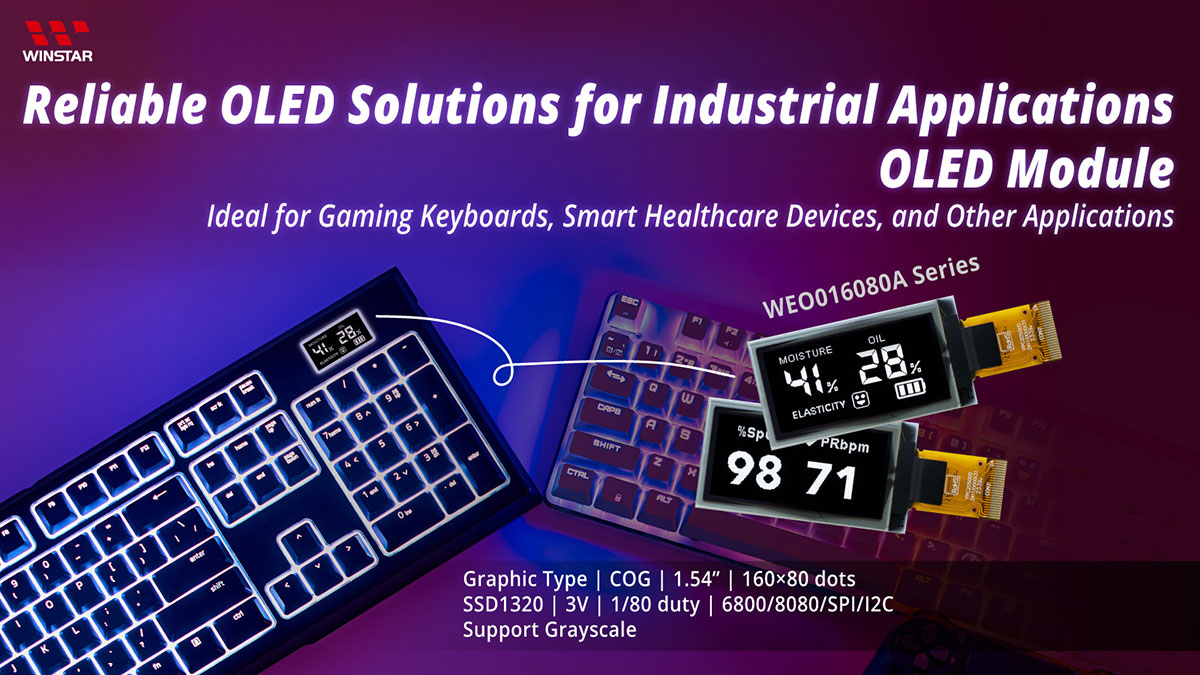
WEO016080A는 해상도가 160x80 도트인 1.54인치 COG 그래픽 OLED 디스플레이입니다. 외형은 43.5 x 22.5 mm이며, 유효 디스플레이 영역은 35.02 x 17.50 mm이며, COG 구조로 인해 두께는 1.41 mm로 매우 얇습니다. SSD1320 IC가 장착되어 있어, 6800/8080 8-bit, 4와이어 SPI, I2C 인터페이스를 지원합니다. 4-bit (16 Levels) 그레이스케일을 제공하며, 대비 비율은 10,000:1을 달성합니다.
논리 전원 공급 전압은 1.65V~3.3V (전형적으로 3.0V), 작동 온도 범위는 -40°C에서 +80°C, 저장 온도 범위는 -40°C에서 +85°C입니다. 네트워킹 제품, USB 테스터, 스마트 시계, 게임 키보드, 혈액 산소 측정기 및 피부 분석기와 같은 스마트 헬스케어 장치 등 다양한 응용 분야에 이상적입니다. WEO016080A의 선명하고 생생한 화면은 디스플레이 품질을 향상시킵니다.
고해상도 (160x80 도트)와 저전력 소비로 성능과 효율을 동시에 요구하는 응용 프로그램에 최적입니다.
Data source ref:WEO016080AWPP3N00000
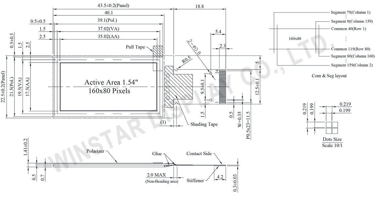
| 항목 | 치수 | 단위 |
|---|---|---|
| 도트 매트릭스 | 160 x 80 Dots | - |
| 모듈 치수 | 43.5 x 22.5 x 1.41 | mm |
| 활성 영역 | 35.02 x 17.50 | mm |
| 도트 크기 | 0.199 x 0.199 | mm |
| 도트 피치 | 0.219 x 0.219 | mm |
| 디스플레이 모드 | 패시브 매트릭스 | |
| 디스플레이 색상 | Monochrome | |
| Drive Duty | 1/80 Duty | |
| 그레이스케일 | 4 bits | |
| 인터페이스 | 6800,8080,4-Wire SPI,I2C | |
| IC | SSD1320 | |
| 크기 | 1.54 인치 | |
| Parameter | 기호 | 최소값 | 대표값. | 최대값 | 단위 |
|---|---|---|---|---|---|
| Supply Voltage for Logic | VDD | -0.3 | - | 4 | V |
| Supply Voltage for Display | VCC | 0 | - | 19 | V |
| 작동 온도 | TOP | -40 | - | +80 | °C |
| 보관 온도 | TSTG | -40 | - | +85 | °C |
| 항목 | 기호 | 조건 | 최소값 | 대표값 | 최대값 | 단위 |
|---|---|---|---|---|---|---|
| Supply Voltage for Logic | VDD | - | 1.65 | 3.0 | 3.3 | V |
| Supply Voltage for Display | VCC | - | 8.0 | 15.0 | 15.5 | V |
| High Level Input | VIH | - | 0.8×VDD | - | VDD | V |
| Low Level Input | VIL | - | 0 | - | 0.2×VDD | V |
| High Level Output | VOH | - | 0.9×VDD | - | VDD | V |
| Low Level Output | VOL | - | 0 | - | 0.1×VDD | V |
| VCC Supply Current | ICC | VDD=3V,VCC=15V Display 50% Pixel ON |
- | 14 | 21 | mA |
| No. | 기호 | 기능 | |||||||||||||||
|---|---|---|---|---|---|---|---|---|---|---|---|---|---|---|---|---|---|
| 1 | N.C. (GND) |
Reserved Pin (Supporting Pin) The supporting pin can reduce the influences from stresses on the function pins. This pin could be connected to external ground as the ESD protection circuit. |
|||||||||||||||
| 2 | VCC | Power Supply for OEL Panel This is the most positive voltage supply pin of the chip. It must be connected to external source. |
|||||||||||||||
| 3~4 | N.C. | Reserved Pin The N.C. pin between function pins are reserved for compatible and flexible design. |
|||||||||||||||
| 5 | BS1 | Communicating Protocol Select These pins are MCU interface selection input. See the following table:
|
|||||||||||||||
| 6 | BS2 | ||||||||||||||||
| 7 | VSS | Ground of Logic Circuit This is a ground pin. It also acts as a reference for the logic pins. It must be connected to external ground. |
|||||||||||||||
| 8 | IREF | Current Reference for Brightness Adjustment This pin is segment current reference pin. A resistor should be connected between this pin and VSS. Set the current at 10μA maximum. |
|||||||||||||||
| 9 | CS# | Chip Select This pin is the chip select input. The chip is enabled for MCU communication only when CS# is pulled low. |
|||||||||||||||
| 10 | RES# | Power Reset for Controller and Driver This pin is reset signal input. When the pin is low, initialization of the chip is executed. Keep this pin pull high during normal operation. |
|||||||||||||||
| 11 | D/C# | Data/Command Control This pin is Data/Command control pin. When the pin is pulled high, the input at D7~D0 is treated as display data. When the pin is pulled low, the input at D7~D0 will be transferred to the command register. In I2C mode, this pin acts as SA0 for slave address selection. |
|||||||||||||||
| 12 | R/W# | Read/Write Select or Write This pin is MCU interface input. When interfacing to a 68XX-series microprocessor, this pin will be used as Read/Write (R/W#) selection input. Pull this pin to “High” for read mode and pull it to “Low” for write mode. When 80XX interface mode is selected, this pin will be the Write (WR#) input. Data write operation is initiated when this pin is pulled low and the CS# is pulled low. When serial mode is selected, this pin must be connected to VSS. |
|||||||||||||||
| 13 | E/RD# | Read/Write Enable or Read This pin is MCU interface input. When interfacing to a 68XX-series microprocessor, this pin will be used as the Enable (E) signal. Read/write operation is initiated when this pin is pulled high and the CS# is pulled low. When connecting to an 80XX-microprocessor, this pin receives the Read (RD#) signal. Data read operation is initiated when this pin is pulled low and CS# is pulled low. When serial mode is selected, this pin must be connected to VSS. |
|||||||||||||||
| 14 | D0 | Host Data Input/Output Bus These pins are bi-directional data bus connecting to the MCU data bus. Unused pins are recommended to tie LOW. When serial interface mode is selected, D2, D1 should be tied together as the serial data input: SDIN, and D0 will be the serial clock input: SCLK. When I2C mode is selected, D2, D1 should be tied together and serve as SDAout, SDAin in application and D0 is the serial clock input, SCL. |
|||||||||||||||
| 15 | D1 | ||||||||||||||||
| 16 | D2 | ||||||||||||||||
| 17 | D3 | ||||||||||||||||
| 18 | D4 | ||||||||||||||||
| 19 | D5 | ||||||||||||||||
| 20 | D6 | ||||||||||||||||
| 21 | D7 | ||||||||||||||||
| 22 | VDD | Power Supply for Logic This is a voltage supply pin. It must be connected to external source. |
|||||||||||||||
| 23 | VCOMH | Voltage Output High Level for COM Signal This pin is the input pin for the voltage output high level for COM signals. A tantalum capacitor should be connected between this pin and VSS. |
|||||||||||||||
| 24 | VCC | Power Supply for OEL Panel This is the most positive voltage supply pin of the chip. It must be connected to external source. |

"모든 쿠키 허용"을 클릭하면 사이트 탐색을 개선하고, 사이트 사용을 분석하며, 마케팅 및 성능 노력에 도움을 주기 위해 쿠키를 귀하의 장치에 저장하는 데 동의한 것으로 간주됩니다. 이 주제에 대한 추가 정보는 당사의 정책에서 확인할 수 있습니다. 개인정보 보호정책