 - WEA012864MX")

우리는 귀하의 프라이버시를 소중히 여깁니다
"모든 쿠키 허용"을 클릭하면 사이트 탐색을 개선하고, 사이트 사용을 분석하며, 마케팅 및 성능 노력에 도움을 주기 위해 쿠키를 귀하의 장치에 저장하는 데 동의한 것으로 간주됩니다. 이 주제에 대한 추가 정보는 당사의 정책에서 확인할 수 있습니다. 개인정보 보호정책

 - WEO012864MX")
 - WEO012864MX")
 - WEO012864MX")
 - WEO012864MX")
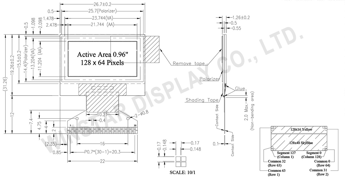
WEO012864MX는 128x64 해상도의 고대비 0.96" OLED 컬러 디스플레이 모듈입니다. 이 모델은 상단 노란색, 하단 스카이 블루의 고정 듀얼 컬러 레이아웃을 사용하여 UI 디자인에 자연스러운 시각적 계층 구조를 제공합니다. 두께 1.26mm의 COG 구조로 설계되어 공간이 제한된 휴대용 기기에 최적화된 프레임리스 솔루션을 제공합니다.
통합된 SSD1306 IC는 내부 VCC 생성을 위한 차지 펌프(DC/DC 컨버터)를 내장하고 있습니다. 이를 통해 3V 단일 전원으로 동작이 가능하며, 외부 부스트 회로를 제거하여 BOM 비용과 PCB 복잡성을 크게 줄일 수 있습니다. 8-bit 6800/8080 병렬, 3/4-wire SPI, I2C 인터페이스를 지원합니다.
| 항목 | 치수 | 단위 |
|---|---|---|
| 도트 매트릭스 | 128 × 64 Dots | - |
| 모듈 치수 | 26.7× 19.26 × 1.26 | mm |
| 활성 영역 | 21.744× 11.204 | mm |
| 도트 크기 | 0.148 × 0.148 | mm |
| 도트 피치 | 0.17 × 0.17 | mm |
| 디스플레이 모드 | 패시브 매트릭스 | |
| 디스플레이 색상 | 듀얼 컬러 (노란색 / 하늘색) | |
| Drive Duty | 1/64 Duty | |
| IC | SSD1306 | |
| 인터페이스 | 6800,8080,SPI,I2C | |
| 크기 (대각선) | 0.96 인치 | |
| Parameter | 기호 | 최소값 | 최대값 | 단위 |
|---|---|---|---|---|
| Supply Voltage for Logic | VDD | 0 | 4 | V |
| Charge Pump Regulator Supply Voltage | VBAT | -0.3 | 5.0 | V |
| Supply Voltage for Display | VCC | 0 | 16.0 | V |
| 작동 온도 | TOP | -40 | +80 | °C |
| 보관 온도 | TSTG | -40 | +85 | °C |
| 항목 | 기호 | 조건 | 최소값 | 대표값 | 최대값 | 단위 |
|---|---|---|---|---|---|---|
| Supply Voltage for Logic | VDD | - | 2.8 | 3.0 | 3.3 | V |
| Supply Voltage for Display (Supplied Externally) |
VCC | - | 11.5 | 12 | 12.5 | V |
| Charge Pump Regulator Supply Voltage | VBAT | - | 3.0 | - | 4.2 | V |
| Charge Pump Output Voltage for Display (Generated by Internal DC/DC) | Charge Pump VCC |
- | 7.0 | 7.5 | - | V |
| Input High Volt. | VIH | - | 0.8×VDD | - | VDD | V |
| Input Low Volt. | VIL | - | 0 | - | 0.2×VDD | V |
| Output High Volt. | VOH | - | 0.9×VDD | - | VDD | V |
| Output Low Volt. | VOL | - | 0 | - | 0.1×VDD | V |
| Operating Current for VCC (50% display ON) (VCC Supplied Externally) |
ICC | VCC =12V | - | 9 | 13.5 | mA |
| 50% check Board operating Current (VCC Generated by Internal DC/DC) | IBAT | - | - | 15 | 25 | mA |
| No. | 기호 | 기능 | ||||||||||||||||||||||||
|---|---|---|---|---|---|---|---|---|---|---|---|---|---|---|---|---|---|---|---|---|---|---|---|---|---|---|
| 1 | N.C. (GND) | Reserved Pin (Supporting Pin) The supporting pins can reduce the influences from stresses on the function pins. These pins must be connected to external ground. |
||||||||||||||||||||||||
| 2 | C2N | Positive Terminal of the Flying Inverting CapacitorNegative Terminal of the Flying Boost CapacitorThe charge-pump capacitors are required between the terminals. They must be floated when the converter is not used. | ||||||||||||||||||||||||
| 3 | C2P | |||||||||||||||||||||||||
| 4 | C1P | |||||||||||||||||||||||||
| 5 | C1N | |||||||||||||||||||||||||
| 6 | VBAT | Power Supply for DC/DC Converter Circuit This is the power supply pin for the internal buffer of the DC/DC voltage converter. It must be connected to external source when the converter is used. It should be connected to VDD when the converter is not used. |
||||||||||||||||||||||||
| 7 | NC | NC | ||||||||||||||||||||||||
| 8 | VSS | Ground of Logic Circuit This is a ground pin. It acts as a reference for the logic pins. It must be connected to external ground. |
||||||||||||||||||||||||
| 9 | VDD | Power Supply for Logic This is a voltage supply pin. It must be connected to external source. |
||||||||||||||||||||||||
| 10 | BS0 | Communicating Protocol Select These pins are MCU interface selection input. See the following table:
|
||||||||||||||||||||||||
| 11 | BS1 | |||||||||||||||||||||||||
| 12 | BS2 | |||||||||||||||||||||||||
| 13 | CS# | Chip Select This pin is the chip select input. The chip is enabled for MCU communication only when CS# is pulled low. |
||||||||||||||||||||||||
| 14 | RES# | Power Reset for Controller and Driver This pin is reset signal input. When the pin is low, initialization of the chip is executed. |
||||||||||||||||||||||||
| 15 | D/C# | Data/Command Control This pin is Data/Command control pin. When the pin is pulled high, the input at D7~D0 is treated as display data. When the pin is pulled low, the input at D7~D0 will be transferred to the command register. For detail relationship to MCU interface signals, please refer to the Timing Characteristics Diagrams. When the pin is pulled high and serial interface mode is selected, the data at SDIN is treated as data. When it is pulled low, the data at SDIN will be transferred to the command register. In I2C mode, this pin acts as SA0 for slave address selection. |
||||||||||||||||||||||||
| 16 | R/W# | Read/Write Select or Write This pin is MCU interface input. When interfacing to a 68XX-series microprocessor, this pin will be used as Read/Write (R/W#) selection input. Pull this pin to “High” for read mode and pull it to “Low” for write mode. When 80XX interface mode is selected, this pin will be the Write (WR#) input. Data write operation is initiated when this pin is pulled low and the CS# is pulled low. |
||||||||||||||||||||||||
| 17 | E/RD# | Read/Write Enable or Read This pin is MCU interface input. When interfacing to a 68XX-series microprocessor, this pin will be used as the Enable (E) signal. Read/write operation is initiated when this pin is pulled high and the CS# is pulled low. When connecting to an 80XX-microprocessor, this pin receives the Read (RD#) signal. Data read operation is initiated when this pin is pulled low and CS# is pulled low. |
||||||||||||||||||||||||
| 18~25 | D0~D7 | Host Data Input/Output Bus These pins are 8-bit bi-directional data bus to be connected to the microprocessor’s data bus. When serial mode is selected, D1 will be the serial data input SDIN and D0 will be the serial clock input SCLK. When I2C mode is selected, D2 & D1 should be tired together and serve as SDAout & SDAin in application and D0 is the serial clock input SCL. |
||||||||||||||||||||||||
| 26 | IREF | Current Reference for Brightness Adjustment This pin is segment current reference pin. A resistor should be connected between this pin and VSS. Set the current lower than 30uA. |
||||||||||||||||||||||||
| 27 | VCOMH | Voltage Output High Level for COM Signal This pin is the input pin for the voltage output high level for COM signals. A capacitor should be connected between this pin and VSS. |
||||||||||||||||||||||||
| 28 | VCC | Power Supply for OEL Panel This is the most positive voltage supply pin of the chip. A stabilization capacitor should be connected between this pin and VSS when the converter is used. It must be connected to external source when the converter is not used. |
||||||||||||||||||||||||
| 29 | VLSS | Ground of Analog Circuit This is an analog ground pin. It should be connected to VSS externally. |
||||||||||||||||||||||||
| 30 | NC (GND) |
Reserved Pin (Supporting Pin) The supporting pins can reduce the influences from stresses on the function pins. These pins must be connected to external ground. |

"모든 쿠키 허용"을 클릭하면 사이트 탐색을 개선하고, 사이트 사용을 분석하며, 마케팅 및 성능 노력에 도움을 주기 위해 쿠키를 귀하의 장치에 저장하는 데 동의한 것으로 간주됩니다. 이 주제에 대한 추가 정보는 당사의 정책에서 확인할 수 있습니다. 개인정보 보호정책