 - WEA012864MX")
我們重視您的隱私
通過點擊「允許所有 Cookie」,代表您同意在您的設備上存儲 Cookie 以增強網站瀏覽體驗、分析網站使用情況並協助我們的行銷和網站效能優化工作。您可以在我們的隱私權政策中找到有關於此的更多資訊。

 - WEO012864MX")
 - WEO012864MX")
 - WEO012864MX")
 - WEO012864MX")
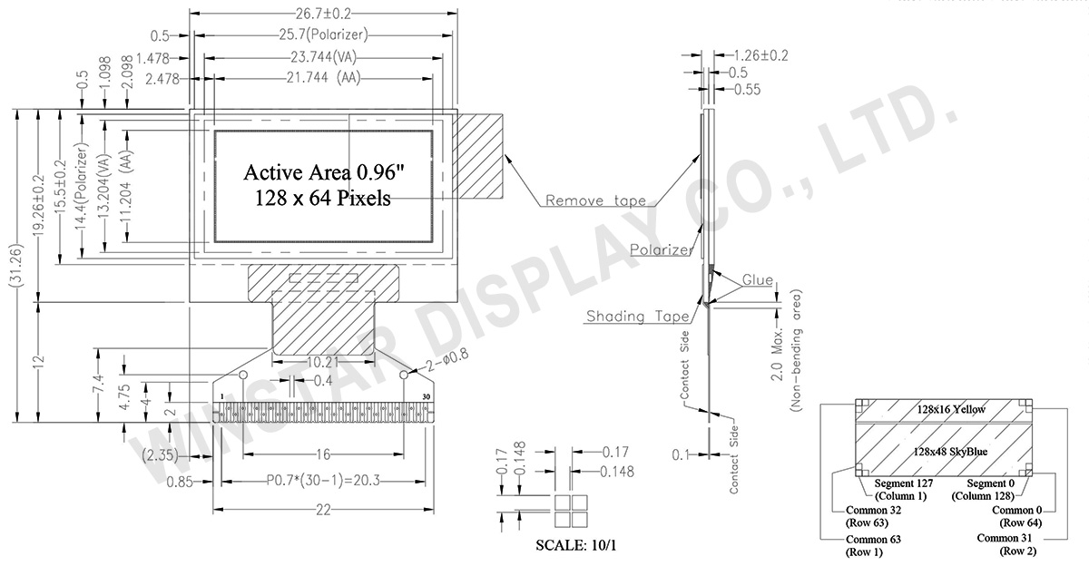
WEO012864MX 是一款高對比的 0.96" OLED 彩色顯示模組,具備 128x64 解析度。此型號採用特殊的固定雙色配置(上方黃色、下方天藍色),為 UI 設計提供直觀的視覺層次。作為 COG (Chip on Glass) 結構的繪圖型 OLED,其厚度僅 1.26mm,是輕量化與空間受限的手持設備之理想無邊框解決方案。
內建的 SSD1306 IC 整合了電荷泵(DC/DC 轉換器),可自行產生 VCC 電壓。這使得彩色 OLED 僅需 3V 單電源即可運作,省去外部升壓電路,大幅降低 BOM 成本與 PCB 複雜度。為了極大化設計彈性,模組支援硬體切換介面,包含 8-bit 6800/8080 並列埠、3/4-wire SPI 與 I2C 通訊協定。
| 項目 | 尺寸 | 單位 |
|---|---|---|
| 點陣 | 128 × 64 Dots | - |
| 模組尺寸 | 26.7× 19.26 × 1.26 | mm |
| 有效區域 | 21.744× 11.204 | mm |
| 點間距 | 0.148 × 0.148 | mm |
| 點大小 | 0.17 × 0.17 | mm |
| 顯示模式 | 被動矩陣 | |
| 發光顏色 | 雙色 (黃色 / 天空藍) | |
| 驅動方式 | 1/64 Duty | |
| IC | SSD1306 | |
| 介面 | 6800,8080,SPI,I2C | |
| 尺寸 | 0.96 吋 | |
| 參數 | 符號 | 最小值 | 最大值 | 單位 |
|---|---|---|---|---|
| 邏輯電源電壓 | VDD | 0 | 4 | V |
| 電荷幫浦穩壓器電源電壓 | VBAT | -0.3 | 5.0 | V |
| 顯示電源電壓 | VCC | 0 | 16.0 | V |
| 工作溫度 | TOP | -40 | +80 | °C |
| 儲存溫度 | TSTG | -40 | +85 | °C |
| 項目 | 符號 | 條件 | 最小值 | 典型值 | 最大值 | 單位 |
|---|---|---|---|---|---|---|
| 邏輯電源電壓 | VDD | - | 2.8 | 3.0 | 3.3 | V |
| 顯示電源電壓 (Supplied Externally) |
VCC | - | 11.5 | 12 | 12.5 | V |
| 電荷幫浦穩壓器電源電壓 | VBAT | - | 3.0 | - | 4.2 | V |
| 顯示器的電荷幫浦輸出電壓 (Generated by Internal DC/DC) | Charge Pump VCC |
- | 7.0 | 7.5 | - | V |
| 輸入高電壓 | VIH | - | 0.8×VDD | - | VDD | V |
| 輸入低電壓 | VIL | - | 0 | - | 0.2×VDD | V |
| 輸出高電壓 | VOH | - | 0.9×VDD | - | VDD | V |
| 輸出低電壓 | VOL | - | 0 | - | 0.1×VDD | V |
| VCC的工作電流 (50% display ON) (VCC Supplied Externally) |
ICC | VCC =12V | - | 9 | 13.5 | mA |
| 50%顯示畫面耗電流 (VCC Generated by Internal DC/DC) | IBAT | - | - | 15 | 25 | mA |
| No. | 符號 | 功能說明 | ||||||||||||||||||||||||
|---|---|---|---|---|---|---|---|---|---|---|---|---|---|---|---|---|---|---|---|---|---|---|---|---|---|---|
| 1 | N.C. (GND) | Reserved Pin (Supporting Pin) The supporting pins can reduce the influences from stresses on the function pins. These pins must be connected to external ground. |
||||||||||||||||||||||||
| 2 | C2N | Positive Terminal of the Flying Inverting CapacitorNegative Terminal of the Flying Boost CapacitorThe charge-pump capacitors are required between the terminals. They must be floated when the converter is not used. | ||||||||||||||||||||||||
| 3 | C2P | |||||||||||||||||||||||||
| 4 | C1P | |||||||||||||||||||||||||
| 5 | C1N | |||||||||||||||||||||||||
| 6 | VBAT | Power Supply for DC/DC Converter Circuit This is the power supply pin for the internal buffer of the DC/DC voltage converter. It must be connected to external source when the converter is used. It should be connected to VDD when the converter is not used. |
||||||||||||||||||||||||
| 7 | NC | NC | ||||||||||||||||||||||||
| 8 | VSS | Ground of Logic Circuit This is a ground pin. It acts as a reference for the logic pins. It must be connected to external ground. |
||||||||||||||||||||||||
| 9 | VDD | Power Supply for Logic This is a voltage supply pin. It must be connected to external source. |
||||||||||||||||||||||||
| 10 | BS0 | Communicating Protocol Select These pins are MCU interface selection input. See the following table:
|
||||||||||||||||||||||||
| 11 | BS1 | |||||||||||||||||||||||||
| 12 | BS2 | |||||||||||||||||||||||||
| 13 | CS# | Chip Select This pin is the chip select input. The chip is enabled for MCU communication only when CS# is pulled low. |
||||||||||||||||||||||||
| 14 | RES# | Power Reset for Controller and Driver This pin is reset signal input. When the pin is low, initialization of the chip is executed. |
||||||||||||||||||||||||
| 15 | D/C# | Data/Command Control This pin is Data/Command control pin. When the pin is pulled high, the input at D7~D0 is treated as display data. When the pin is pulled low, the input at D7~D0 will be transferred to the command register. For detail relationship to MCU interface signals, please refer to the Timing Characteristics Diagrams. When the pin is pulled high and serial interface mode is selected, the data at SDIN is treated as data. When it is pulled low, the data at SDIN will be transferred to the command register. In I2C mode, this pin acts as SA0 for slave address selection. |
||||||||||||||||||||||||
| 16 | R/W# | Read/Write Select or Write This pin is MCU interface input. When interfacing to a 68XX-series microprocessor, this pin will be used as Read/Write (R/W#) selection input. Pull this pin to “High” for read mode and pull it to “Low” for write mode. When 80XX interface mode is selected, this pin will be the Write (WR#) input. Data write operation is initiated when this pin is pulled low and the CS# is pulled low. |
||||||||||||||||||||||||
| 17 | E/RD# | Read/Write Enable or Read This pin is MCU interface input. When interfacing to a 68XX-series microprocessor, this pin will be used as the Enable (E) signal. Read/write operation is initiated when this pin is pulled high and the CS# is pulled low. When connecting to an 80XX-microprocessor, this pin receives the Read (RD#) signal. Data read operation is initiated when this pin is pulled low and CS# is pulled low. |
||||||||||||||||||||||||
| 18~25 | D0~D7 | Host Data Input/Output Bus These pins are 8-bit bi-directional data bus to be connected to the microprocessor’s data bus. When serial mode is selected, D1 will be the serial data input SDIN and D0 will be the serial clock input SCLK. When I2C mode is selected, D2 & D1 should be tired together and serve as SDAout & SDAin in application and D0 is the serial clock input SCL. |
||||||||||||||||||||||||
| 26 | IREF | Current Reference for Brightness Adjustment This pin is segment current reference pin. A resistor should be connected between this pin and VSS. Set the current lower than 30uA. |
||||||||||||||||||||||||
| 27 | VCOMH | Voltage Output High Level for COM Signal This pin is the input pin for the voltage output high level for COM signals. A capacitor should be connected between this pin and VSS. |
||||||||||||||||||||||||
| 28 | VCC | Power Supply for OEL Panel This is the most positive voltage supply pin of the chip. A stabilization capacitor should be connected between this pin and VSS when the converter is used. It must be connected to external source when the converter is not used. |
||||||||||||||||||||||||
| 29 | VLSS | Ground of Analog Circuit This is an analog ground pin. It should be connected to VSS externally. |
||||||||||||||||||||||||
| 30 | NC (GND) |
Reserved Pin (Supporting Pin) The supporting pins can reduce the influences from stresses on the function pins. These pins must be connected to external ground. |

通過點擊「允許所有 Cookie」,代表您同意在您的設備上存儲 Cookie 以增強網站瀏覽體驗、分析網站使用情況並協助我們的行銷和網站效能優化工作。您可以在我們的隱私權政策中找到有關於此的更多資訊。