


우리는 귀하의 프라이버시를 소중히 여깁니다
"모든 쿠키 허용"을 클릭하면 사이트 탐색을 개선하고, 사이트 사용을 분석하며, 마케팅 및 성능 노력에 도움을 주기 위해 쿠키를 귀하의 장치에 저장하는 데 동의한 것으로 간주됩니다. 이 주제에 대한 추가 정보는 당사의 정책에서 확인할 수 있습니다. 개인정보 보호정책


WEO012864AE는 1.54인치 COG 128×64 그래픽 OLED 디스플레이 모듈로, CH1116 IC가 내장되어 있습니다. I2C, 4선 SPI, 6800 및 8080 병렬 인터페이스를 지원합니다. 로직 전원 공급 전압은 일반적으로 3 V이며, 디스플레이 전원 공급 전압은 12.5 V(대표값), 구동 듀티는 1/64입니다.
WEO012864AE 시리즈는 24핀 및 30핀 ZIF FPC 옵션을 제공합니다. 맞춤형 FPC 설계도 요청 시 가능합니다.
이 모듈은 IoT 시스템, 스마트 홈 애플리케이션, 금융 POS, 지능형 기기, 에너지 시스템, 통신 시스템, 의료 기기 등에 적합합니다. 동작 온도 범위는 -40 °C ~ +80 °C이며, 보관 온도 범위는 -40 °C ~ +85 °C입니다.
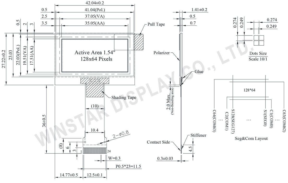
| 항목 | 치수 | 단위 |
|---|---|---|
| 도트 매트릭스 | 128 × 64 | dots |
| 모듈 치수 | 42.04 × 27.22 × 1.41 | mm |
| 활성 영역 | 35.05 × 17.51 | mm |
| 도트 크기 | 0.249 × 0.249 | mm |
| 도트 피치 | 0.274 × 0.274 | mm |
| 디스플레이 모드 | 패시브 매트릭스 (Passive Matrix) | |
| 디스플레이 색 | Monochrome | |
| Drive Duty | 1/64 Duty | |
| IC | CH1116 | |
| 인터페이스 | 6800,8080,4-wire SPI,I2C | |
| 크기 | 1.54 인치 | |
| Parameter | 기호 | 최소값 | 최대값 | 단위 |
|---|---|---|---|---|
| Supply Voltage for Logic | VDD | -0.3 | 3.6 | V |
| Supply Voltage for Display | VCC | 0 | 14.5 | V |
| 작동 온도 | TOP | -40 | +80 | °C |
| 보관 온도 | TSTG | -40 | +85 | °C |
| 항목 | 기호 | 조건 | 최소값 | 대표값 | 최대값 | 단위 |
|---|---|---|---|---|---|---|
| Supply Voltage for Logic | VDD1 | - | 1.65 | 3.0 | 3.3 | V |
| Supply Voltage for Display | VPP | - | 6.4 | 12.5 | 13.0 | V |
| High Level Input | VIH | - | 0.8×VDD1 | - | VDD1 | V |
| Low Level Input | VIL | - | VSS | - | 0.2×VDD1 | V |
| High Level Output | VOH | - | 0.8×VDD1 | - | VDD1 | V |
| Low Level Output | VOL | - | VSS | - | 0.2×VDD1 | V |
| Display 50% Pixel on | IPP | VPP =12.5V | - | 8 | 12 | mA |
| No. | 기호 | 기능 | |||||||||||||||
|---|---|---|---|---|---|---|---|---|---|---|---|---|---|---|---|---|---|
| 1 | NC(GND) | No connection | |||||||||||||||
| 2 | VSS | Ground. | |||||||||||||||
| 3 | VSS | Ground. | |||||||||||||||
| 4 | NC | No connection | |||||||||||||||
| 5 | VDD1 | Power supply input | |||||||||||||||
| 6 | IM1 | These are the MPU interface mode select pads.
(1) 0 is connected to VSS (2) 1 is connected to VDD1 |
|||||||||||||||
| 7 | IM2 | ||||||||||||||||
| 8 | CS# | This pad is the chip select input. When CS# = “L”, then the chip select becomes active, and data/command I/O is enabled. | |||||||||||||||
| 9 | RES# | This is a reset signal input pad. When RES# is set to “L”, the settings are initialized. The reset operation is performed by the RES# signal level. | |||||||||||||||
| 10 | A0 | This is the Data/Command control pad that determines whether the data bits are data or a command. A0 = “H”: the inputs at D0 to D7 are treated as display data. A0 = “L”: the inputs at D0 to D7 are transferred to the command registers. In I2C interface, this pad serves as SA0 to distinguish the different address of OLED driver. |
|||||||||||||||
| 11 | WR# (R/W#) |
This is a MPU interface input pad. When connected to an 8080 MPU, this is active LOW. This pad connects to the 8080 MPU WR# signal. The signals on the data bus are latched at the rising edge of the WR# signal. When connected to a 6800 Series MPU: This is the read/write control signal input terminal. When R/W#= “H”: Read. When R/W#= “L”: Write. |
|||||||||||||||
| 12 | E/RD# | This is a MPU interface input pad. When connected to an 8080 series MPU, it is active LOW. This pad is connected to the RD# signal of the 8080 series MPU, and the data bus is in an output status when this signal is “L”. When connected to a 6800 series MPU, this is active HIGH. This is used as an enable clock input of the 6800 series MPU. When RD# = “H”: Enable. When RD# = “L”: Disable. |
|||||||||||||||
| 13-20 | D0~D7 | This is an 8-bit bi-directional data bus that connects to an 8-bit or 16-bit standard MPU data bus. When the serial interface is selected, then D0 serves as the serial clock input pad (SCL) and D1 serves as the serial data input pad (SI). At this time, D2 to D7 are set to high impedance. When the I2C interface is selected, then D0 serves as the serial clock input pad (SCL) and D1 serves as the serial data input pad (SDAI). At this time, D2 to D7 are set to high impedance. |
|||||||||||||||
| 21 | IREF | This is a segment current reference pad. A resistor should be connected between this pad and VSS. Set the current at 18.75uA. | |||||||||||||||
| 22 | VCOMH | This is a pad for the voltage output high level for common signals. A capacitor should be connected between this pad and VSS. |
|||||||||||||||
| 23 | VPP | OLED panel power supply. It could be supplied externally. A capacitor should be connected between this pad and VSS. |
|||||||||||||||
| 24 | NC(GND) | No connection |

"모든 쿠키 허용"을 클릭하면 사이트 탐색을 개선하고, 사이트 사용을 분석하며, 마케팅 및 성능 노력에 도움을 주기 위해 쿠키를 귀하의 장치에 저장하는 데 동의한 것으로 간주됩니다. 이 주제에 대한 추가 정보는 당사의 정책에서 확인할 수 있습니다. 개인정보 보호정책