Home Products TFT Display High Brightness TFT Display WF121FSYAPLNB0

12.1-inch TFT Capacitive Display with 10-Point Multi-Touch

Model No. WF121FSYAPLNB0

►Size : 12.1"
►Resolution : 1280 x 800 dots
►View Direction : IPS
►Interface : LVDS
►Driver IC : --
►Control-Board : No
►Brightness(cd/m²) : 800
►Frame Through Hole : No
►Touch Screen : Projected Capacitive Touch Panel (PCAP)
►Detect Point : 10 Fingers
►Operating Temperature : -20~+70℃

Description

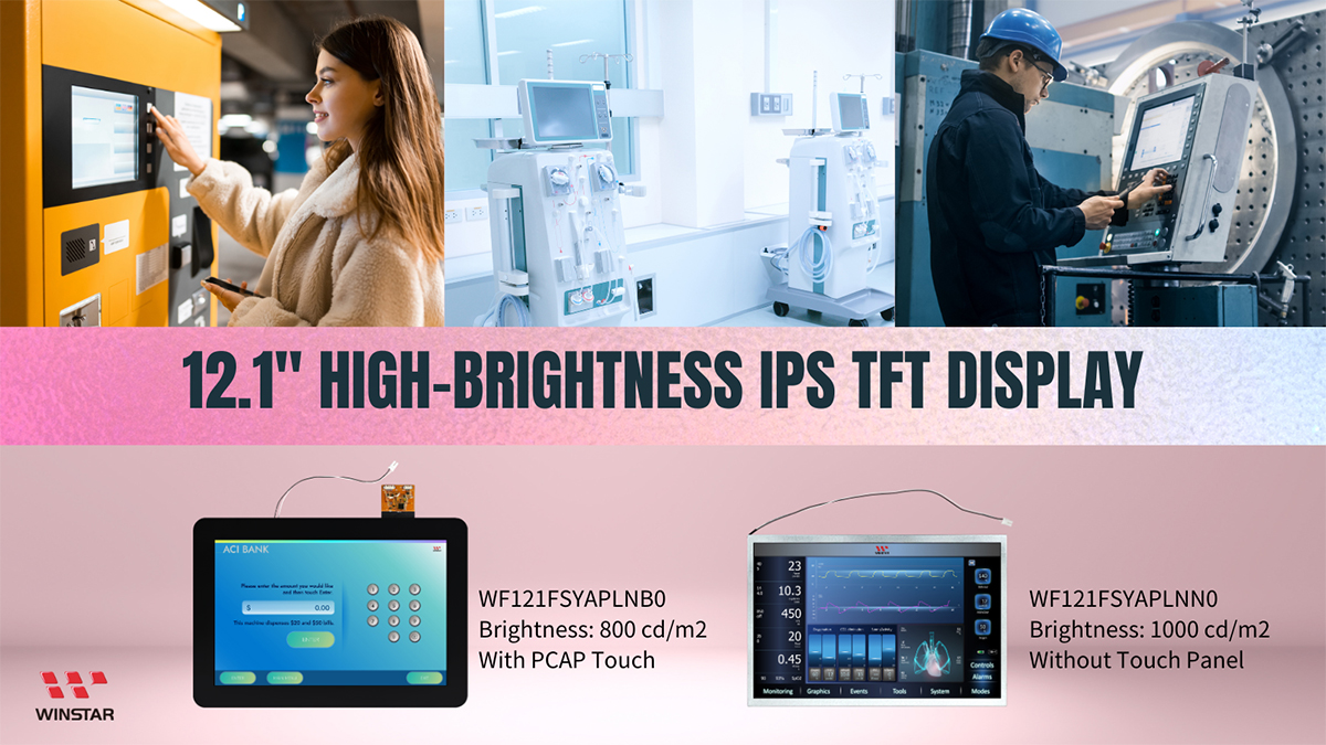
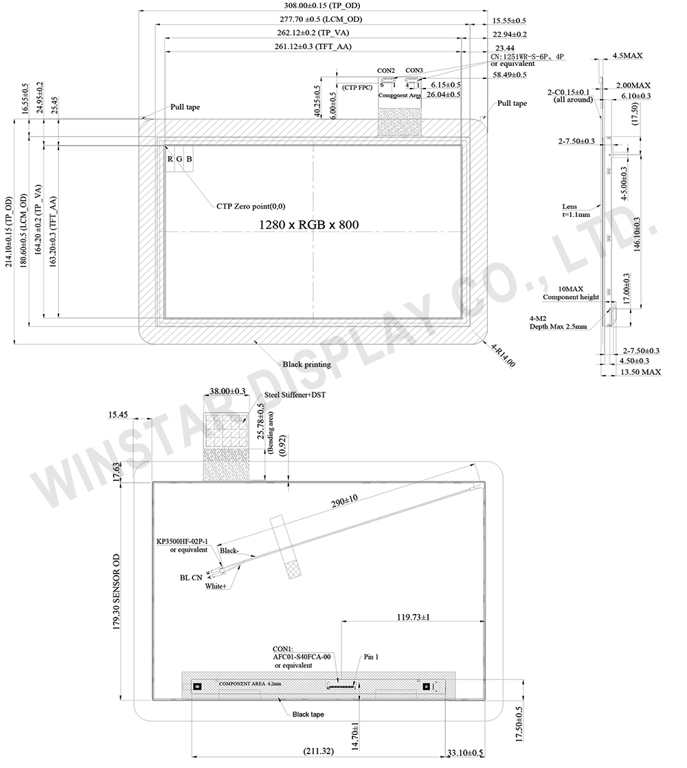
The WF121FSYAPLNB0 is a 12.1-inch high-brightness TFT capacitive display** designed for applications requiring precise visual clarity and responsive touch interaction. With a resolution of 1280 × 800 pixels (WXGA) and a 16:9 aspect ratio, this capacitive touchscreen display delivers sharp, detailed images even in bright lighting conditions, making it suitable for both indoor and outdoor use.

Featuring an LVDS interface, the module ensures stable and reliable data transmission. The integrated capacitive touch functionality is driven by the ILI2132 driver IC, supporting USB and I²C interfaces, and providing 10-point multi-touch capability. Its high sensitivity and accuracy allow smooth operation with multiple simultaneous touches, making this TFT capacitive display ideal for interactive systems such as medical devices, ATMs, industrial control panels, and self-service kiosks.

With a peak brightness of 800 nits and a contrast ratio of 1200:1, the module delivers vibrant and lifelike visuals. The IPS technology provides wide viewing angles of 85° in all directions, maintaining consistent color fidelity from multiple viewing positions. The capacitive touchscreen display ensures that user interaction is intuitive and precise.

Designed for reliability, the WF121FSYAPLNB0 operates within a temperature range of -20°C to +70°C, guaranteeing stable performance across varied environmental conditions.

Reliable Displays, Empowering Innovation Across Every Industry

DRAWING

Capacitive Touchscreen Display, Capacitive Display, TFT Capacitive Display - WF121FSYAPLNB0

SPECIFICATIONS

General Specifications

Item Dimension Unit
Size 12.1 inch
Dot Matrix 1280 x 3(RGB) x 800 dots
Module dimension 308.0 x 214.1 x 13.5 mm
Active area 261.12 x 163.2 mm
Pixel pitch 0.204 x 0.204 mm
LCD type TFT, Normally Black ,Transmissive
Backlight Type LED, Normally White
View Angle 85/85/85/85 (IPS)
Interface LVDS
Aspect Ratio 16:9
PCAP Driver IC ILI2132 or equivalent
PCAP Resolution 16384*16384
PCAP Interface USB (I2C available)
PCAP FW Version 0x07.0x00.0x00.0x00.0x02.0x00.0x00.0x00
Touch Panel Projected Capacitive Touch Panel (PCAP)
Surface Treatment Glare

Absolute Maximum Ratings

Item Symbol Min Typ Max Unit
Operating Temperature TOP -20 +70
Storage Temperature TST -30 +80

Electrical Characteristics

Typical Operation Conditions

Item Symbol Min Typ Max Unit
Supply voltage VDD 3.0 3.3 3.6 V
Current Consumption
All Black
Logic ICC+IIN - 440 660 mA
Analog
Supply CTP VDDT(3.3V) 3.0 3.3 3.6 V
IDDT(3.3V) - 87 135 mA
VDDT(5V) - 5.0 - V
IDDT(5V) - 92 140 mA
 

Backlight Driving Conditions

Parameter Symbol Min. Typ. Max. Unit
LED current ILED - 360 - mA
LED voltage VLED+ 22.8 24.08 27.2 V
LED Life Time   - 50,000 - Hr

Interface Pin Function

1.LCM PIN Definition

Pin No. Symbol Function
1 NC No contact
2 VDD Power supply VDDIN=3.3V
3 VDD
4 VDD
5 NC No contact
6 GND Digital power
7 GND Digital ground
8 RIN0- LVDS Negative data signal (-)
9 RIN0+ LVDS Negative data signal (+)
10 GND GND
11 RIN1- LVDS Negative data signal (-)
12 RIN1+ LVDS Negative data signal (+)
13 GND GND
14 RIN2- LVDS Negative data signal (-)
15 RIN2+ LVDS Negative data signal (+)
16 GND GND
17 LVDS_CLK- LVDS Negative CLK signal (-)
18 LVDS_CLK+ LVDS Negative CLK signal (+)
19 GND GND
20 RIN3- LVDS Negative data signal (-)
21 RIN3+ LVDS Negative data signal (+)
22 GND GND
23 NC No contact
24 NC No contact
25 GND GND
26 NC No contact
27 NC No contact
28 GND GND
29 NC No contact
30 NC No contact
31 GND GND
32 GND GND
33 GND GND
34-40 NC No contact
 

2.BL CN

Pin No. Symbol Function
1 White(VLED+) LED_ Anode
2 Black(VLED-) LED_ Cathode
 

3.CON2

Pin No. Symbol Function
1 VDDT(3.3V) Power supply
2 SDA I2C data input and output
3 SCL I2C clock input I2C clock input
4 RST External Reset, Low is active
5 INT External interrupt to the host
6 VSS Ground for analog circuit
 

4. CON3

Pin No. Symbol Function
1 VDDT(5V) Power supply
2 D- Data -
3 D+ Data +
4 VSS System ground

Related Products

Recently Viewed

go top
close

We value your privacy

By clicking "Allow All Cookies", you agree to the storing of cookies on your device to enhance site navigation, analyse site usage, and assist in our marketing and performance efforts. You can find further information this subject in our policy.

We value your privacy

Winstar and certain third parties use cookies on www.winstar.com.tw. The details regarding the types of
cookies, their purpose and the third parties involved are described below and in our Cookie Policy.
Please click on “Allow All” to consent to our usage of cookies in order to have the best possible
experience on our websites. You can also set your preferences or reject cookies (except for strictly
necessary cookies).

Manage Consent Preferences

Always Active
Essential Cookies

These cookies are essential in order to enable you to move around the website and use its
features, such as setting your privacy preferences, logging in or filling in forms.

Analytics Cookies

Also known as “statistics cookies,” these cookies collect information about how you use a website, like which pages you visited and which links you clicked on. See Detail