Home Products HMI Display Development Board WL0F00088000BGXAANA00

8.8 Inch Bar Type Edge AI Vision Development Board

Model No. WL0F00088000BGXAANA00

►LCD Display Size: 8.8 inch
►Resolution: 1920×480 dots
►View Direction: 85/85/85/85(IPS)
►Communication Interface: CAN FD, RS485, RS232, Ethernet, USB-C, UART, SPI, I2C, GPIO
►Camera Interface: MIPI CSI-2 / Parallel
►Touch Panel: Capacitive Touch Panel
►Brightness(cd/m²): 450
►Operating Voltage: 9-36V
►Support ST TouchGFX
►64 MB External Flash

Description

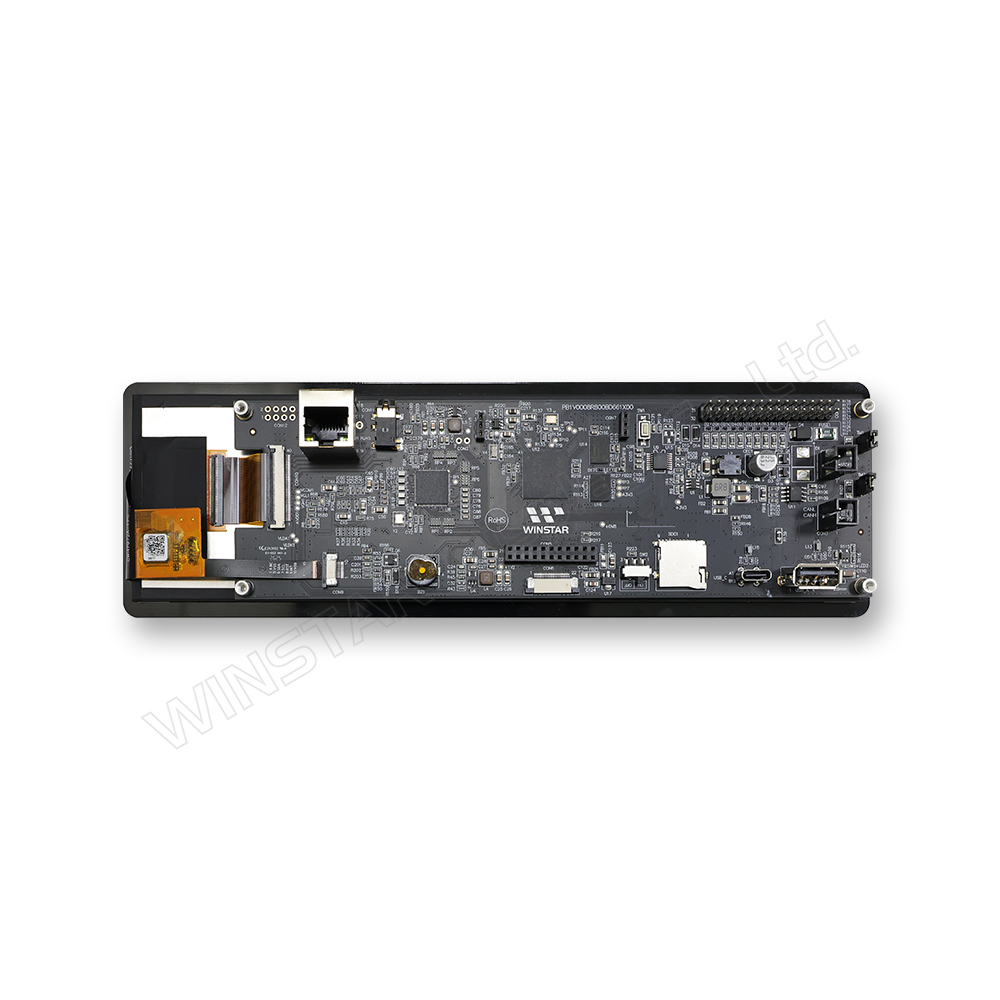
WL0F00088000BGXAANA00 is an 8.8-inch bar-type STM32 development board powered by the STM32N657 MCU. Featuring the Neural-ART NPU with AI acceleration of up to 600 GOPS at 1 GHz, the board is designed for edge AI vision and embedded system development. It supports on-device AI inference, enabling visual data processing without relying on a cloud connection.

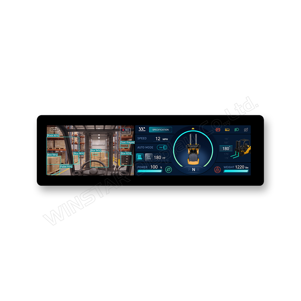
The development board integrates an 8.8-inch IPS TFT LCD with a 1920x480 resolution, 85/85/85/85-degree wide viewing angles, and a projected capacitive touch panel (PCAP). Its bar-type display format is suitable for space-constrained applications such as smart home appliances, off-highway vehicle dashboards, and narrow industrial control panels.

Designed for edge AI vision development, the board provides MIPI CSI-2 and parallel camera interfaces for camera connectivity. When paired with the B-CAMS-IMX camera unit, the platform can perform on-device visual recognition and AI inference for applications such as anomaly detection, object recognition, and human detection.

WL0F00088000BGXAANA00 provides multiple communication interfaces, including CAN FD, RS485, RS232, Ethernet, USB-C, UART, SPI, I2C, and GPIO. It also features 32 MB RAM, 64 MB external Flash memory, a 9V to 36V wide input voltage range, and support for ST TouchGFX. The board operates from -20℃ to +70℃ and can be stored from -30℃ to +80℃.

As an ST Authorized Partner, WINSTAR develops display and embedded hardware solutions based on the STM32 ecosystem. This development board combines STM32N657 processing, AI acceleration, camera connectivity, and a bar-type touch display in a single development platform for edge AI vision and embedded system development.

Note: Reliability testing is currently in progress, and product samples are under preparation. Sample availability is expected in approximately 2 to 3 months.

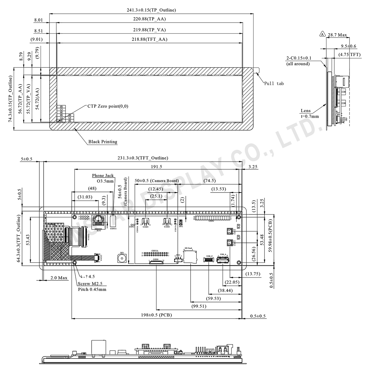
DRAWING

WL0F00088000BGXAANA00 Contour Drawing

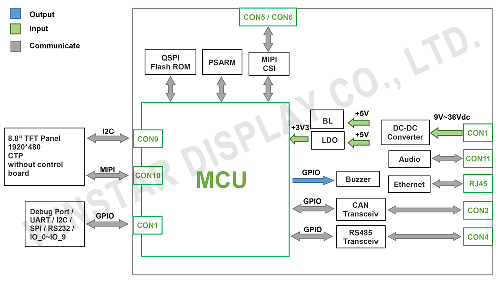
Block Diagram

WL0F00088000BGXAANA00 - Block Diagram

SPECIFICATIONS

General Specifications

Item Standard Value Unit
Operating voltage 9V~36V dynamic Vdc
Communication Interface  CANFD / RS485 / RS232 / UART / LAN / SPI / I2C / USB N/A
MCU  STM32N657 N/A
RAM 32 MB
Flash Memory 64 MB
LCD display size 8.8 inch
Dot Matrix 1920 x RGB x 480(TFT) dot
Module dimension 241.3(W) x 74.3(H) x 28.7(D) mm
Active area 218.88 (H) x 54.72(V) mm
Pixel pitch 0.114(W) x 0.114(H) mm
Brightness Min:350; Typ:450 cd/m2
LCD type TFT, Normally Black, Transmissive
View Direction 85/85/85/85
Aspect Ratio 1:4 (Bar Type)
Touch Panel With Projected Capacitive Touch Panel (PCAP)
Surface Glare

Absolute Maximum Ratings

Item Symbol Min Typ Max Unit
Operating Temperature TOP -20 +70
Storage Temperature TST -30 +80

Electrical Characteristics

Item Symbol Condition Min Typ Max Unit
Supply Voltage VIN 9 12 36 V
Supply LCM Current I(mA) 420 300 105 mA

BOM

Item Description
LCM WF88BTYA8MNG10#
PCBA PB4V0008R800BD661X00

Interface Pin Function

CON1 definition:

Pin Symbol Function Remark
1 VIN Power supply input V+ Input
2 +3V3 3.3V power for JTAG interface Output
3 VIN Power supply input V+ Input
4 SWCLK CLK pin for JTAG interface I/O
5 GND Power supply GND input GND
6 GND Power supply GND input GND
7 GND Power supply GND input GND
8 SWDIO Data pin for JTAG interface I/O
9 SPI_CS SPI Chip select interface Input
10 NRST Reset pin for JTAG interface Input
11 SPI_CLK SPI Clock interface I/O
12 BOOT0 Power supply GND input Input
13 SPI_MOSI SPI MOSI interface Output
14 IO_0 Timer, Event, I/O PB5
15 SPI_MISO SPI MISO interface Input
16 IO_1 ADC, Timer, Event, I/O PA9
17 I2C_SDA I2C SDA interface I/O
18 IO_2 ADC, Timer, Event, I/O PA10
19 I2C_SCL I2C SCL interface I/O
20 IO_3 ADC, Timer, Event, I/O PB10
21 UART1_TX UART TX interface Output
22 IO_4 DAC, Timer, Event, I/O PB3
23 UART1_RX UART RX interface Input
24 IO_5 PWM, Timer, Event, I/O PE7
25 UART2_TX UART TX interface Output
26 IO_6 PWM, Timer, Event, I/O PE8
27 UART2_RX UART RX interface Input
28 IO_7 PWM, Timer, Event, I/O PE9
29 RS232_TX RS232 TX interface Output
30 IO_8 PWM, Timer, Event, I/O PE10
31 RS232_RX RS232 RX interface Input
32 IO_9 PWM, Timer, Event, I/O PE12
 

CON3 definition:

Pin Symbol Function Remark
1 CAN_H CAN BUS High interface I/O
2 CAN_L CAN BUS Low interface I/O
 

CON4 definition:

Pin Symbol Function Remark
1 RS485_A RS485 A interface I/O
2 RS485_B RS485 B interface I/O
 

CON6 definition:

Pin Symbol Function Remark
1 GND Power GND GND
2 CSI_D0_N MIPI CSI D0 negative signal I/O
3 CSI_D0_P MIPI CSI D0 positive signal I/O
4 GND Power GND GND
5 CSI_D1_N MIPI CSI D1 negative signal I/O
6 CSI_D1_P MIPI CSI D1 positive signal I/O
7 GND Power GND GND
8 CSI_CLK_N MIPI CSI clock negative signal I/O
9 CSI_CLK_P MIPI CSI clock positive signal I/O
10 GND Power GND GND
11 TOF_LPn TOF LPn interface I/O
12 TOF_INT TOF INT interface Input
13 GND Power GND GND
14 IMU_INT1 IMU INT1 interface Input
15 IMU_INT2 IMU INT2 interface Input
16 GND Power GND GND
17 CAM_NRST Camera Reset Input
18 CAM_EN Camera Enable Input
19 GND Power GND GND
20 CAM_SCL Camera SCL interface I/O
21 CAM_SDA Camera SDA interface I/O
22 VDD_CAM Power supply +3.3V Input
go top
close

We value your privacy

By clicking "Allow All Cookies", you agree to the storing of cookies on your device to enhance site navigation, analyse site usage, and assist in our marketing and performance efforts. You can find further information this subject in our policy.

We value your privacy

Winstar and certain third parties use cookies on www.winstar.com.tw. The details regarding the types of
cookies, their purpose and the third parties involved are described below and in our Cookie Policy.
Please click on “Allow All” to consent to our usage of cookies in order to have the best possible
experience on our websites. You can also set your preferences or reject cookies (except for strictly
necessary cookies).

Manage Consent Preferences

Always Active
Essential Cookies

These cookies are essential in order to enable you to move around the website and use its
features, such as setting your privacy preferences, logging in or filling in forms.

Analytics Cookies

Also known as “statistics cookies,” these cookies collect information about how you use a website, like which pages you visited and which links you clicked on. See Detail