
我們重視您的隱私
通過點擊「允許所有 Cookie」,代表您同意在您的設備上存儲 Cookie 以增強網站瀏覽體驗、分析網站使用情況並協助我們的行銷和網站效能優化工作。您可以在我們的隱私權政策中找到有關於此的更多資訊。


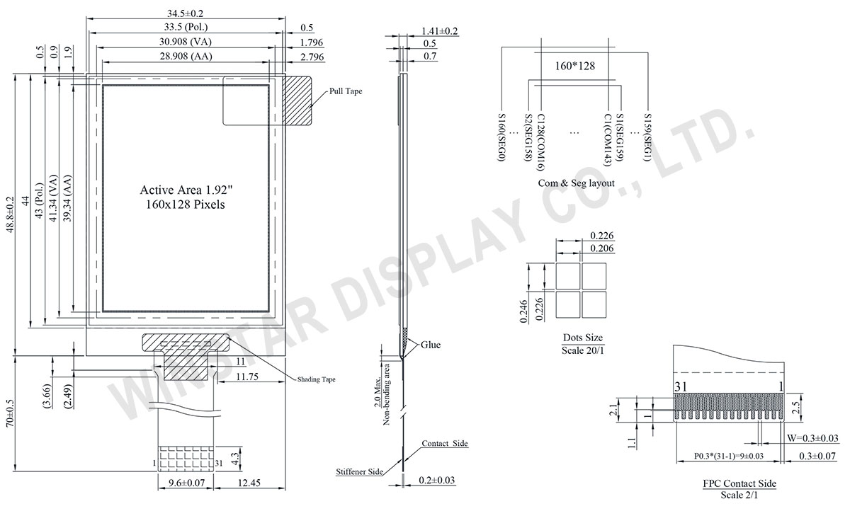
WEO160128B系列是160x128解析度的COG繪圖型OLED顯示模組,對角線為1.92吋。 此型號內建CH1120 IC 支援6800/8080並列介面和I2C/4線SPI串列介面。邏輯電壓為3V,顯示電壓為12V ,OLED模組優點具有高對比度10,000:1,所搭配的IC可支援4-bit灰階。此系列1.92吋COG OLED模組適用於醫療應用、智能家居應用、智能建築設備(包括家庭和辦公室)以及用於管理照明或暖器等設備的控制面板、智能手錶、運動手錶。此模組工作溫度為-40℃~+80℃;儲存溫度為-40℃~+85℃。
| 項目 | 規格 | 單位 |
|---|---|---|
| 解析度 | 128 × 160 | Dots |
| 模組尺寸 | 34.5 × 48.8 × 1.41 | mm |
| 有效區域 | 28.908 × 39.34 | mm |
| 像素大小 | 0.206 × 0.226 | mm |
| 像素間距 | 0.226 × 0.246 | mm |
| 顯示模式 | 被動矩陣 | |
| 顯示顏色 | 單色 | |
| 驅動方式 | 1/128 Duty | |
| IC | CH1120 | |
| 介面 | 6800, 8080, SPI, I2C | |
| 尺寸 | 1.92 吋 | |
| 參數 | 符號 | 最小值 | 最大值 | 單位 |
|---|---|---|---|---|
| 邏輯電源電壓 | VDD | -0.3 | 3.5 | V |
| 顯示電源電壓 | VPP | -0.3 | 15.0 | V |
| 工作溫度 | TOP | -40 | +80 | °C |
| 儲存溫度 | TSTG | -40 | +85 | °C |
| 項目 | 符號 | 條件 | 最小值 | 典型值 | 最大值 | 單位 |
|---|---|---|---|---|---|---|
| 邏輯電源電壓 | VDD | - | 1.65 | 3.0 | 3.5 | V |
| 邏輯電源電壓 | VPP | - | 11.5 | 12.0 | 12.5 | V |
| 輸入高電壓 | VIH | - | 0.8xVDD | - | VDD | V |
| 輸入低電壓 | VIL | - | VSS | - | 0.2xVDD | V |
| 輸出高電壓 | VOH | IOH=-0.5mA | 0.8xVDD | - | VDD | V |
| 輸出低電壓 | VOL | IOL=0.5mA | VSS | - | 0.2xVDD | V |
| Display 50% Pixel on | IPP | VPP=12V | - | 25 | 37.5 | mA |
| No. | 符號 | 功能 | ||||||||||||||||||||||||
|---|---|---|---|---|---|---|---|---|---|---|---|---|---|---|---|---|---|---|---|---|---|---|---|---|---|---|
| 1 | NC | No connection | ||||||||||||||||||||||||
| 2 | VPP | This is the most positive voltage supply pad of the chip. It should be supplied externally. |
||||||||||||||||||||||||
| 3 | VSEGM | This is a segment pre-charge voltage. A capacitor can be connected between this pad and VSS if necessary. When external capacitor Is not used, this pin should be kept NC. |
||||||||||||||||||||||||
| 4 | VCOMH | This is a pad for the voltage output high level for common signals. A capacitor should be connected between this pad and VSS. |
||||||||||||||||||||||||
| 5 | VSL | Discharge voltage level pad. This pad should be connected to resistor and diode externally. |
||||||||||||||||||||||||
| 6 | NC | No connection | ||||||||||||||||||||||||
| 7 | IREF | This is a segment current reference pad. A resistor should be connected between this pad and VSS. . |
||||||||||||||||||||||||
| 8 | VPP | This is the most positive voltage supply pad of the chip. It should be supplied externally. |
||||||||||||||||||||||||
| 9 | NC | No connection | ||||||||||||||||||||||||
| 10 | VSS | Ground for logic and analog. This pad should be connected to GND externally. | ||||||||||||||||||||||||
| 11 | VCL | This is a common voltage reference pad. This pad should be connected to VSS externally. |
||||||||||||||||||||||||
| 12 | VDD | Power supply for logic and input/output | ||||||||||||||||||||||||
| 13 | IM0 | These are the MPU interface mode select pads.
|
||||||||||||||||||||||||
| 14 | IM1 | |||||||||||||||||||||||||
| 16 | IM2 | |||||||||||||||||||||||||
| 15 | VDD | Power supply for logic and input/output | ||||||||||||||||||||||||
| 17 | CS | This pad is the chip select input. When CSB = "L", then the chip select becomes active, and data command I/O is enabled. When in I2C interface, this pin is not used, so it must be connected to "L". | ||||||||||||||||||||||||
| 18 | RES | This is a reset signal input pad. When RESB is set to "L", the settings are initialized. The reset operation is performed by the RESB signal level. This pin internal pull high. | ||||||||||||||||||||||||
| 19 | A0 | This is the Data/Command control pad that determines whether the data bits are data or a command. A0 = "H ": the inputs at D0 to D7 are treated as display data. A0 = "L ": the inputs at D0 to D7 are transferred to the command registers. In I2C interface, this pad serves as SA0 to distinguish the different address of OLED driver. When in 3-wire interface, this pin is not used, so it must be connected to "L ". |
||||||||||||||||||||||||
| 20 | WR | This is a MPU interface input pad. When connected to an 8080 MPU, this is active LOW. This pad connects to the 8080 MPU WR signal. The signals on the data bus are latched at the rising edge of the WR signal. When connected to a 6800 Series MPU: This is the read/write control signal input terminal. When R/W = "H ": Read. When R/W = "L ": Write. When in 3-wire.4-wire & I2C interface, this pin is not used, so it must be connected to "L ". |
||||||||||||||||||||||||
| 21 | RD | This is a MPU interface input pad. When connected to an 8080 series MPU, it is active LOW. This pad is connected to the RD signal of the 8080 series MPU, and the data bus is in an output status when this signal is "L". When connected to a 6800 series MPU, this is active HIGH. This is used as an enable clock input of the 6800 series MPU. When in 3-wire.4-wire & I2C interface, this pin is not used, so it must be connected to "L". |
||||||||||||||||||||||||
| 22 | D0 | This is an 8-bit bi-directional data bus that connects to an 8-bit or 16-bit standard MPU data bus. When the serial interface(SPI) and I2C is selected, then D0 serves as the serial clock input pad (SCL) and D1 serves as the serial data input pad (SI). At this time, D2 to D7 are set to high impedance. D7~D2 is recommended to connect the VDD or GND. It is also allowed to leave D7~D2 unconnected. |
||||||||||||||||||||||||
| 23 | D1 | |||||||||||||||||||||||||
| 24 | D2 | |||||||||||||||||||||||||
| 25 | D3 | |||||||||||||||||||||||||
| 26 | D4 | |||||||||||||||||||||||||
| 27 | D5 | |||||||||||||||||||||||||
| 28 | D6 | |||||||||||||||||||||||||
| 29 | D7 | |||||||||||||||||||||||||
| 30 | NC | No connection | ||||||||||||||||||||||||
| 31 | VPP | This is the most positive voltage supply pad of the chip. It should be supplied externally. |

通過點擊「允許所有 Cookie」,代表您同意在您的設備上存儲 Cookie 以增強網站瀏覽體驗、分析網站使用情況並協助我們的行銷和網站效能優化工作。您可以在我們的隱私權政策中找到有關於此的更多資訊。