
我們重視您的隱私
通過點擊「允許所有 Cookie」,代表您同意在您的設備上存儲 Cookie 以增強網站瀏覽體驗、分析網站使用情況並協助我們的行銷和網站效能優化工作。您可以在我們的隱私權政策中找到有關於此的更多資訊。


| 項目 | 標準尺寸 | 單位 |
|---|---|---|
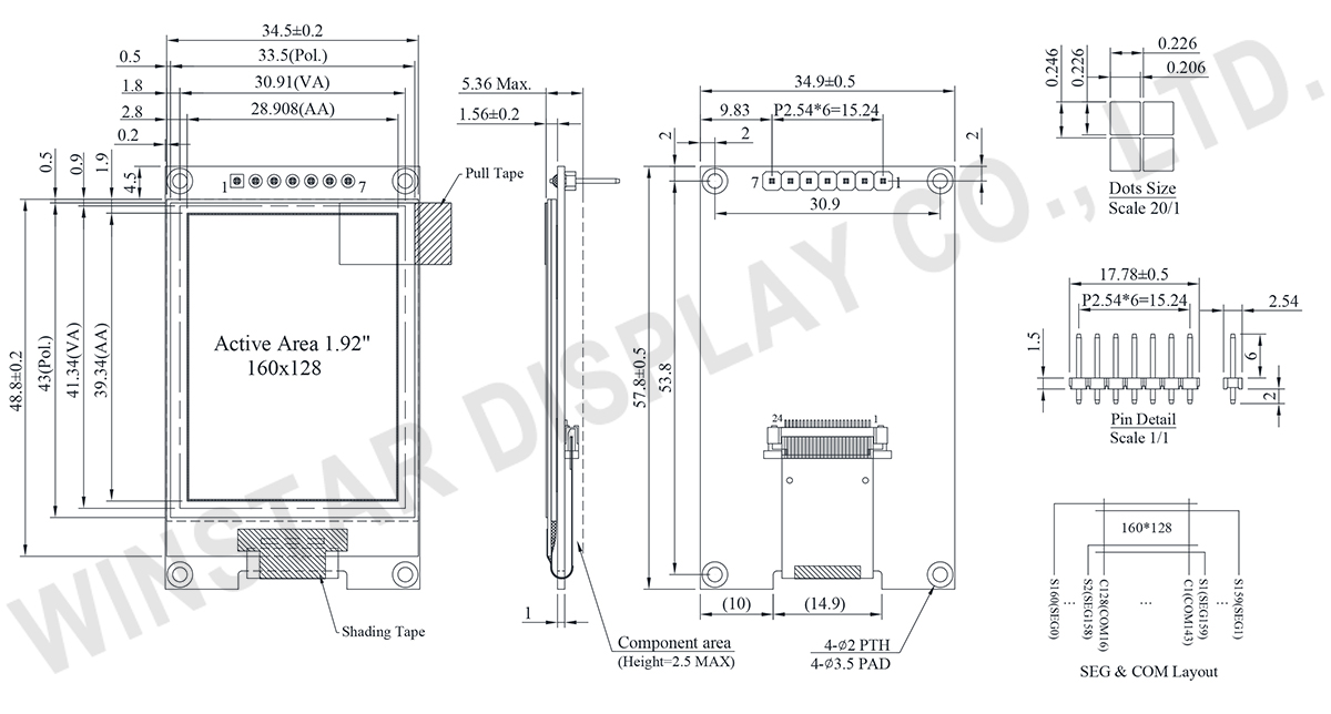
| 點陣(解析度) | 160 x 128 | - |
| 模組尺寸 | 34.90 x 57.80 x 5.36(Max) | mm |
| 有效區域 | 28.908 x 39.34 | mm |
| 點大小 | 0.206 x 0.226 | mm |
| 點間距 | 0.226 x 0.246 | mm |
| 顯示模式 | 被動矩陣 | |
| 發光顏色 |
單色 |
|
| 驅動方式 | 1/128 Duty | |
| 灰階 | 4 bits | |
| OLED IC | CH1120 | |
| OLED 介面 | SPI | |
| 顯示尺寸(對角線) | 1.92 吋 | |
| 項目 | 符號 | 最小值 | 最大值 | 單位 |
|---|---|---|---|---|
| 邏輯電源電壓 | VDD | -0.3 | 6.5 | V |
| 工作溫度 | TOP | -40 | +80 | ℃ |
| 儲存溫度 | TSTG | -40 | +85 | ℃ |
| 項目 | 符號 | 條件 | 最小值 | 典型值 | 最大值 | 單位 |
|---|---|---|---|---|---|---|
| 邏輯電源電壓 | VDD | - | 3.0 | 3.3 | 5.2 | V |
| 輸入高電壓 | VIH | - | 0.8VDD | - | VDD | V |
| 輸入低電壓 | VIL | - | VSS | - | 0.2VDD | V |
| 輸出高電壓 | VOH | IOH=-0.5mA | 0.8VDD | - | VDD | V |
| 輸出低電壓 | VOL | IOL=0.5mA | VSS | - | 0.2VDD | V |
| Display 50% Pixel on | IDD | VDD=3.3V | - | 160 | 240 | mA |
| Pin No. | 符號 | 功能 |
|---|---|---|
| 1 | GND | Ground for logic and analog. This pad should be connected to GND externally. |
| 2 | VDD | Power supply for logic and input/output |
| 3 | SCL | serial clock input |
| 4 | SI | serial data input |
| 5 | ___ RES |
This is a reset signal input pad. When RES is set to “L”, the settings are initialized. The reset operation is performed by the RES signal level. This pin internal pull high. |
| 6 | A0 | This is the Data/Command control pad that determines whether the data bits are data or a command. A0 = “H”: the inputs at D0 and D1 are treated as display data. A0 = “L”: the inputs at D0 and D1 are transferred to the command registers. |
| 7 | __ CS |
This pad is the chip select input. When CS = “L”, then the chip select becomes active, and data/command I/O is enabled. |

通過點擊「允許所有 Cookie」,代表您同意在您的設備上存儲 Cookie 以增強網站瀏覽體驗、分析網站使用情況並協助我們的行銷和網站效能優化工作。您可以在我們的隱私權政策中找到有關於此的更多資訊。