
我们重视您的隐私
通过点击「允许所有 Cookie」,代表您同意在您的设备上存储 Cookie 以增强网站浏览体验、分析网站使用情况并协助我们的营销和网站效能优化工作。您可以在我们的隐私权政策中找到有关于此的更多信息。


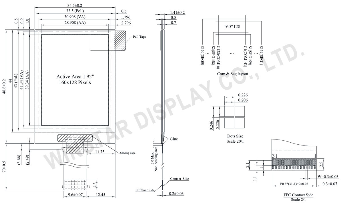
WEO160128B系列是160x128分辨率的COG绘图型OLED显示模块,对角线为1.92吋。 此型号内建CH1120 IC 支持6800/8080并列接口和I2C/4线SPI串行接口。逻辑电压为3V,显示电压为12V ,OLED模块优点具有高对比度度10,000:1,所搭配的IC可支持4-bit灰阶。此系列1.92吋COG OLED模块适用于医疗应用、智能家居应用、智能建筑设备(包括家庭和办公室)以及用于管理照明或暖器等设备的控制面板、智能手表、运动手表。此模块工作温度为-40℃~+80℃;储存温度为-40℃~+85℃。
| 项目 | 规格 | 单位 |
|---|---|---|
| 分辨率 | 128 × 160 | Dots |
| 模块尺寸 | 34.5 × 48.8 × 1.41 | mm |
| 有效区域 | 28.908 × 39.34 | mm |
| 像素大小 | 0.206 × 0.226 | mm |
| 像素间距 | 0.226 × 0.246 | mm |
| 显示模式 | 被动矩阵 | |
| 显示颜色 | 单色 | |
| 驱动方式 | 1/128 Duty | |
| IC | SH1108 | |
| 接口 | 6800, 8080, SPI, I2C | |
| 尺寸 | 1.92 寸 | |
| 参数 | 符号 | 最小值 | 最大值 | 单位 |
|---|---|---|---|---|
| 逻辑电源电压 | VDD | -0.3 | 3.6 | V |
| 显示电源电压 | VPP | -0.3 | 17.0 | V |
| 工作温度 | TOP | -40 | +80 | °C |
| 储存温度 | TSTG | -40 | +85 | °C |
| 项目 | 符号 | 条件 | 最小值 | 典型值 | 最大值 | 单位 |
|---|---|---|---|---|---|---|
| 逻辑电源电压 | VDD | - | 1.65 | 3.0 | 3.5 | V |
| 逻辑电源电压 | VPP | - | 11.5 | 12.0 | 12.5 | V |
| 输入高电压 | VIH | - | 0.8xVDD | - | VDD | V |
| 输入低电压 | VIL | - | VSS | - | 0.2xVDD | V |
| 输出高电压 | VOH | IOH=-0.5mA | 0.8xVDD | - | VDD | V |
| 输出低电压 | VOL | IOL=0.5mA | VSS | - | 0.2xVDD | V |
| 50% Check Board Operating Current for VPP | IPP | VPP=12V | - | 23.0 | 35.0 | mA |
| No. | 符号 | 功能 | ||||||||||||||||||||||||
|---|---|---|---|---|---|---|---|---|---|---|---|---|---|---|---|---|---|---|---|---|---|---|---|---|---|---|
| 1 | NC | No connection | ||||||||||||||||||||||||
| 2 | VPP | This is the most positive voltage supply pad of the chip. It should be supplied externally. |
||||||||||||||||||||||||
| 3 | VSEGM | This is a pad for the voltage output level for segment pre-charge. A capacitor should be connected between this pad and VSS. |
||||||||||||||||||||||||
| 4 | VCOMH | This is a pad for the voltage output high level for common signals. A capacitor should be connected between this pad and VSS. |
||||||||||||||||||||||||
| 5 | VSL | This is a segment voltage reference pad. A capacitor should be connected between this pad and VSS. |
||||||||||||||||||||||||
| 6 | NC | No connection | ||||||||||||||||||||||||
| 7 | IREF | This is a segment current reference pad. A resistor should be connected between this pad and VSS. Set the current at 15.625uA. |
||||||||||||||||||||||||
| 8 | VPP | This is the most positive voltage supply pad of the chip. It should be supplied externally. |
||||||||||||||||||||||||
| 9 | NC | No connection | ||||||||||||||||||||||||
| 10 | VSS | Ground for analog, logic & buffer respectively. | ||||||||||||||||||||||||
| 11 | VCL | This is a common voltage reference pad. This pad should be connected to VSS externally. |
||||||||||||||||||||||||
| 12 | VDD | 1.65 - 3.5V power supply input pad for logic. | ||||||||||||||||||||||||
| 13 | IM0 | These are the MPU interface mode select pads.
|
||||||||||||||||||||||||
| 14 | IM1 | |||||||||||||||||||||||||
| 16 | IM2 | |||||||||||||||||||||||||
| 15 | VDD | 1.65 - 3.5Vpower supply input pad | ||||||||||||||||||||||||
| 17 | CS | This pad is the chip select input. When CS = “L”, then the chip select becomes active, and data command I/O is enabled. | ||||||||||||||||||||||||
| 18 | RES | This is a reset signal input pad. When RES is set to “L”, the settings are initialized. The reset operation is performed by the RES signal level. | ||||||||||||||||||||||||
| 19 | A0 | This is the Data/Command control pad that determines whether the data bits are data or a command. A0 = “H”: the inputs at D0 to D7 are treated as display data. A0 = “L”: the inputs at D0 to D7 are transferred to the command registers. In I2C interface, this pad serves as SA0 to distinguish the different address of OLED driver. |
||||||||||||||||||||||||
| 20 | WR | This is a MPU interface input pad. When connected to an 8080 MPU, this is active LOW. This pad connects to the 8080 MPU WR signal. The signals on the data bus are latched at the rising edge of the WR signal. When connected to a 6800 Series MPU: This is the read/write control signal input terminal. When WR = “H”: Read. When WR = “L”: Write. |
||||||||||||||||||||||||
| 21 | RD | This is a MPU interface input pad. When connected to an 8080 series MPU, it is active LOW. This pad is connected to the RD signal of the 8080 series MPU, and the data bus is in an output status when this signal is “L”. When connected to a 6800 series MPU, this is active HIGH. This is used as an enable clock input of the 6800 series MPU. |
||||||||||||||||||||||||
| 22 | D0 | This is an 8-bit bi-directional data bus that connects to an 8-bit or 16-bit standard MPU data bus. When the serial interface is selected, then D0 serves as the serial clock input pad (SCL) and D1 serves as the serial data input pad (SI). At this time, D2 to D7 are set to high impedance. When the I2C interface is selected, then D0 serves as the serial clock input pad (SCL) and D1 serves as the serial data input pad (SDA). At this time, D2 to D7 are set to high impedance. |
||||||||||||||||||||||||
| 23 | D1 | |||||||||||||||||||||||||
| 24 | D2 | |||||||||||||||||||||||||
| 25 | D3 | |||||||||||||||||||||||||
| 26 | D4 | |||||||||||||||||||||||||
| 27 | D5 | |||||||||||||||||||||||||
| 28 | D6 | |||||||||||||||||||||||||
| 29 | D7 | |||||||||||||||||||||||||
| 30 | NC | No connection | ||||||||||||||||||||||||
| 31 | VPP | This is the most positive voltage supply pad of the chip. It should be supplied externally. |

通过点击「允许所有 Cookie」,代表您同意在您的设备上存储 Cookie 以增强网站浏览体验、分析网站使用情况并协助我们的营销和网站效能优化工作。您可以在我们的隐私权政策中找到有关于此的更多信息。