
私たちはあなたのプライバシーを大切にします
「すべてのクッキーを許可」をクリックすると、サイトのナビゲーションを向上させ、サイト使用状況を分析し、マーケティングおよびパフォーマンスの取り組みを支援するために、クッキーをデバイスに保存することに同意したことになります。この件に関する詳細情報は、ポリシーをご覧ください。プライバシーポリシー


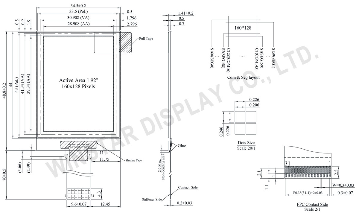
WEO160128Bは、サイズは1.92インチの160x128 COGグラフィック表示の有機EL液晶(OLED)ディスプレイモジュールです。WEO160128Bは、サイズは1.92インチの160x128 COGグラフィック表示の有機EL液晶(OLED)ディスプレイモジュールです。CH1120のICを搭載していて、6800/8080 パラレル インターフェイス、I2C、および 4 線 SPI シリアル インターフェイスをサポートします。モジュールの電源電圧は3V、ディスプレイ用電源電圧は12Vで、4ビット階調をサポートします。コントラスト比は10,000:1(代表値)、解像度160×128ピクセルです。このOLEDモジュールは医療用途、スマートホーム、インテリビル(住宅やオフィス)、照明や暖房などの制御設備に適用します。動作温度範囲は-40℃~+80℃、保管温度範囲は-40℃~+85℃です。
| 項目 | 仕様 | 単位 |
|---|---|---|
| ドットマトリックス(解像度) | 128 × 160 | Dots |
| 外形寸法 | 34.5 × 48.8 × 1.41 | mm |
| 有効表示エリア | 28.908 × 39.34 | mm |
| ドットサイズ | 0.206 × 0.226 | mm |
| ドットピッチ | 0.226 × 0.246 | mm |
| 表示モード | パッシブマトリクス | |
| 発光色 | モノクロ | |
| 駆動方法 | 1/128 Duty | |
| IC | CH1120 | |
| インターフェイス | 6800, 8080, SPI, I2C | |
| サイズ | 1.92 インチ | |
| パラメーター | 記号 | 最小値 | 最大値 | 単位 |
|---|---|---|---|---|
| ロジック電源電圧 | VDD | -0.3 | 3.5 | V |
| Display電源電圧 | VPP | -0.3 | 15.0 | V |
| 操作温度 | TOP | -40 | +80 | °C |
| 保存温度 | TSTG | -40 | +85 | °C |
| 項目 | 記号 | 条件 | 最小値 | 典型値 | 最大値 | 単位 |
|---|---|---|---|---|---|---|
| ロジック電源電圧 | VDD | - | 1.65 | 3.0 | 3.5 | V |
| Display電源電圧 | VPP | - | 11.5 | 12.0 | 12.5 | V |
| 入力電圧(High) | VIH | - | 0.8xVDD | - | VDD | V |
| 入力電圧(Low) | VIL | - | VSS | - | 0.2xVDD | V |
| 出力電圧(High) | VOH | IOH=-0.5mA | 0.8xVDD | - | VDD | V |
| 出力電圧(Low) | VOL | IOL=0.5mA | VSS | - | 0.2xVDD | V |
| Display 50% Pixel on | IPP | VPP=12V | - | 25 | 37.5 | mA |
| No. | 記号 | 説明 | ||||||||||||||||||||||||
|---|---|---|---|---|---|---|---|---|---|---|---|---|---|---|---|---|---|---|---|---|---|---|---|---|---|---|
| 1 | NC | No connection | ||||||||||||||||||||||||
| 2 | VPP | This is the most positive voltage supply pad of the chip. It should be supplied externally. |
||||||||||||||||||||||||
| 3 | VSEGM | This is a segment pre-charge voltage. A capacitor can be connected between this pad and VSS if necessary. When external capacitor Is not used, this pin should be kept NC. |
||||||||||||||||||||||||
| 4 | VCOMH | This is a pad for the voltage output high level for common signals. A capacitor should be connected between this pad and VSS. |
||||||||||||||||||||||||
| 5 | VSL | Discharge voltage level pad. This pad should be connected to resistor and diode externally. |
||||||||||||||||||||||||
| 6 | NC | No connection | ||||||||||||||||||||||||
| 7 | IREF | This is a segment current reference pad. A resistor should be connected between this pad and VSS. . |
||||||||||||||||||||||||
| 8 | VPP | This is the most positive voltage supply pad of the chip. It should be supplied externally. |
||||||||||||||||||||||||
| 9 | NC | No connection | ||||||||||||||||||||||||
| 10 | VSS | Ground for logic and analog. This pad should be connected to GND externally. | ||||||||||||||||||||||||
| 11 | VCL | This is a common voltage reference pad. This pad should be connected to VSS externally. |
||||||||||||||||||||||||
| 12 | VDD | Power supply for logic and input/output | ||||||||||||||||||||||||
| 13 | IM0 | These are the MPU interface mode select pads.
|
||||||||||||||||||||||||
| 14 | IM1 | |||||||||||||||||||||||||
| 16 | IM2 | |||||||||||||||||||||||||
| 15 | VDD | Power supply for logic and input/output | ||||||||||||||||||||||||
| 17 | CS | This pad is the chip select input. When CSB = "L", then the chip select becomes active, and data command I/O is enabled. When in I2C interface, this pin is not used, so it must be connected to "L". | ||||||||||||||||||||||||
| 18 | RES | This is a reset signal input pad. When RESB is set to "L", the settings are initialized. The reset operation is performed by the RESB signal level. This pin internal pull high. | ||||||||||||||||||||||||
| 19 | A0 | This is the Data/Command control pad that determines whether the data bits are data or a command. A0 = "H ": the inputs at D0 to D7 are treated as display data. A0 = "L ": the inputs at D0 to D7 are transferred to the command registers. In I2C interface, this pad serves as SA0 to distinguish the different address of OLED driver. When in 3-wire interface, this pin is not used, so it must be connected to "L ". |
||||||||||||||||||||||||
| 20 | WR | This is a MPU interface input pad. When connected to an 8080 MPU, this is active LOW. This pad connects to the 8080 MPU WR signal. The signals on the data bus are latched at the rising edge of the WR signal. When connected to a 6800 Series MPU: This is the read/write control signal input terminal. When R/W = "H ": Read. When R/W = "L ": Write. When in 3-wire.4-wire & I2C interface, this pin is not used, so it must be connected to "L ". |
||||||||||||||||||||||||
| 21 | RD | This is a MPU interface input pad. When connected to an 8080 series MPU, it is active LOW. This pad is connected to the RD signal of the 8080 series MPU, and the data bus is in an output status when this signal is "L". When connected to a 6800 series MPU, this is active HIGH. This is used as an enable clock input of the 6800 series MPU. When in 3-wire.4-wire & I2C interface, this pin is not used, so it must be connected to "L". |
||||||||||||||||||||||||
| 22 | D0 | This is an 8-bit bi-directional data bus that connects to an 8-bit or 16-bit standard MPU data bus. When the serial interface(SPI) and I2C is selected, then D0 serves as the serial clock input pad (SCL) and D1 serves as the serial data input pad (SI). At this time, D2 to D7 are set to high impedance. D7~D2 is recommended to connect the VDD or GND. It is also allowed to leave D7~D2 unconnected. |
||||||||||||||||||||||||
| 23 | D1 | |||||||||||||||||||||||||
| 24 | D2 | |||||||||||||||||||||||||
| 25 | D3 | |||||||||||||||||||||||||
| 26 | D4 | |||||||||||||||||||||||||
| 27 | D5 | |||||||||||||||||||||||||
| 28 | D6 | |||||||||||||||||||||||||
| 29 | D7 | |||||||||||||||||||||||||
| 30 | NC | No connection | ||||||||||||||||||||||||
| 31 | VPP | This is the most positive voltage supply pad of the chip. It should be supplied externally. |

「すべてのクッキーを許可」をクリックすると、サイトのナビゲーションを向上させ、サイト使用状況を分析し、マーケティングおよびパフォーマンスの取り組みを支援するために、クッキーをデバイスに保存することに同意したことになります。この件に関する詳細情報は、ポリシーをご覧ください。プライバシーポリシー