
私たちはあなたのプライバシーを大切にします
「すべてのクッキーを許可」をクリックすると、サイトのナビゲーションを向上させ、サイト使用状況を分析し、マーケティングおよびパフォーマンスの取り組みを支援するために、クッキーをデバイスに保存することに同意したことになります。この件に関する詳細情報は、ポリシーをご覧ください。プライバシーポリシー


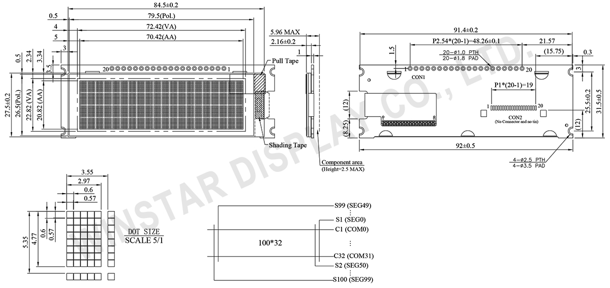
型番 WEA002004C
►タイプ: キャラクタ表示タイプが
►結構: COG+PCB
►20文字x4行
►IC:SSD1311
►3.3V/5V電源電圧
►1/32 duty
►インターフェース: 6800,8080,SPI,I2C
►発光色: 白色 / 黄色
WEA002004CはCOG構造のキャラクター有機ELディスプレイで、PCB基板を搭載しております。対角寸法2.89インチ 、 20 文字 x 4 行で、10,000:1高コントラストのため、はっきりと表示させて見やすいです。SSD1311 ICを内蔵し、6800/8080 4ビット/8ビットパラレルと4線 SPI/I2C のインターフェースをサポート致します。 デューティは 1/32 で、ロジック電源電圧 は5Vで、3.3Vも選択可能です。WEA002004CはASCII、英語、ヨーロッパ語および日本語のフォントを提供致します。
WEA002004Cの基板に固定用の取り付け穴付きのため、簡単にお得意先の設備と製品に実装できます。
WEA002004C 有機ELモジュールはスマートホームアプリケーション、医療機器、スマートコントロール、メーターなどに適しております。 操作温度範囲は -40℃ ~+80℃で、保存温度範囲は-40℃ ~ +85℃です。
Data source ref: WEA002004CWPP3N00000
| 項目 | サイズ | 単位 |
|---|---|---|
| 表示形式 | 20文字x4行 | - |
| モジュールサイズ | 92.0 x 31.5 x 5.96 Max. | mm |
| 表示エリア | 72.42 x 22.82 | mm |
| アクティブエリア | 70.42 x 20.82 | mm |
| ドットサイズ | 0.57 x 0.57 | mm |
| ドットピッチ | 0.60 x 0.60 | mm |
| 文字サイズ | 2.97 x 4.77 | mm |
| 文字ピッチ | 3.55 x 5.35 | mm |
| LCDタイプ | OLED , モノクロ | |
| Duty | 1/32 | |
| IC | SSD1311 | |
| インターフェイス | 6800, 8080, SPI, I2C | |
| サイズ | 2.89 インチ | |
| 項目 | 記号 | 最小値 | 最大値 | 単位 |
|---|---|---|---|---|
| 操作温度 | TOP | -40 | +80 | °C |
| 保存温度 | TST | -40 | +85 | °C |
| ロジック電源電圧 | VDD-VSS | -0.3 | 3.6 | V |
| 項目 | 記号 | 条件 | 最小値 | 典型値 | 最大値 | 単位 |
|---|---|---|---|---|---|---|
| ロジック電源電圧 | VDD-VSS | - | 2.8 | 3.0 | 3.3 | V |
| 高レベル入力電圧 | VIH | - | 0.8xVDD | - | VDD | V |
| 低レベル入力電圧 | VIL | - | GND | - | 0.2xVDD | V |
| 高レベル出力電圧 | VOH | IOH=-0.5mA | 0.8xVDD | - | VDD | V |
| 低レベル出力電圧 | VOL | IOL=0.5mA | GND | - | 0.2xVDD | V |
| Display 50% Pixel on | IDD | VDD=3V | - | 110 | 220 | mA |
| Pin No. | 記号 | Pin Type | 説明 | ||||||||||||||||||
|---|---|---|---|---|---|---|---|---|---|---|---|---|---|---|---|---|---|---|---|---|---|
| 1 | VSS | P | Ground | ||||||||||||||||||
| 2 | VDD | P | Power supply and power supply for interface logic level. | ||||||||||||||||||
| 3 | REGVDD | I | This pin is pulled LOW, internal VDD regulator is disabled (Low voltage I/O application). | ||||||||||||||||||
| 4 | D/C# | I | This pin is Data/Command control pin connecting to the MCU. When the pin is pulled HIGH, the data at D[7:0] will be interpreted as data. When the pin is pulled LOW, the data at D[7:0] will be transferred to a command register. In I2C mode, this pin acts as SA0 for slave address selection. When serial interface is selected, this pin must be connected to VSS. |
||||||||||||||||||
| 5 | R/W# (WR#) | I | This pin is read / write control input pin connecting to the MCU interface. When 6800 interface mode is selected, this pin will be used as Read/Write (R/W#) selection input. Read mode will be carried out when this pin is pulled HIGH and write mode when LOW. When 8080 interface mode is selected, this pin will be the Write (WR#) input. Data write operation is initiated when this pin is pulled LOW and the chip is selected. When serial or I2C interface is selected, this pin must be connected to VSS. |
||||||||||||||||||
| 6 | E/RD# | I | This pin is MCU interface input. When 6800 interface mode is selected, this pin will be used as the Enable (E) signal. Read/write operation is initiated when this pin is pulled HIGH and the chip is selected. When 8080 interface mode is selected, this pin receives the Read (RD#) signal. Read operation is initiated when this pin is pulled LOW and the chip is selected. When serial or I2C interface is selected, this pin must be connected to VSS. |
||||||||||||||||||
| 7 | D0 | I/O | These pins are bi-directional data bus connecting to the MCU data bus. Unused pins are recommended to tie LOW. When serial interface mode is selected, D0 will be the serial clock input: SCLK; D1 will be the serial data input: SID and D2 will be the serial data output: SOD. When I2C mode is selected, D2, D1 should be tied together and serve as SDAout, SDAin in application and D0 is the serial clock input, SCL. |
||||||||||||||||||
| 8 | D1 | ||||||||||||||||||||
| 9 | D2 | ||||||||||||||||||||
| 10 | D3 | ||||||||||||||||||||
| 11 | D4 | ||||||||||||||||||||
| 12 | D5 | ||||||||||||||||||||
| 13 | D6 | ||||||||||||||||||||
| 14 | D7 | ||||||||||||||||||||
| 15 | CS# | I | This pin is the chip select input connecting to the MCU. The chip is enabled for MCU communication only when CS# is pulled LOW (active LOW). In I2C mode, this pin must be connected to VSS. |
||||||||||||||||||
| 16 | RES# | I | This pin is reset signal input. When the pin is pulled LOW, initialization of the chip is executed. Keep this pin pull HIGH during normal operation. |
||||||||||||||||||
| 17 | BS0 | I | setting as described in the following table. BS2, BS1 and BS0 are pin select. Bus Interface selection
(1) 0 is connected to VSS (2) 1 is connected to VDD |
||||||||||||||||||
| 18 | BS1 | ||||||||||||||||||||
| 19 | BS2 | ||||||||||||||||||||
| 20 | VSS (FRGnd) |
P | Ground |
Search keyword: oled 20x4, 20x4 oled

「すべてのクッキーを許可」をクリックすると、サイトのナビゲーションを向上させ、サイト使用状況を分析し、マーケティングおよびパフォーマンスの取り組みを支援するために、クッキーをデバイスに保存することに同意したことになります。この件に関する詳細情報は、ポリシーをご覧ください。プライバシーポリシー