


我們重視您的隱私
通過點擊「允許所有 Cookie」,代表您同意在您的設備上存儲 Cookie 以增強網站瀏覽體驗、分析網站使用情況並協助我們的行銷和網站效能優化工作。您可以在我們的隱私權政策中找到有關於此的更多資訊。


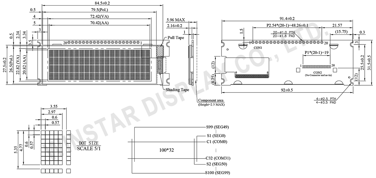
型號 WEA002004C
►類型: 字元
►結構: COG+PCB
►20字x4行
►IC:SSD1311
►3.3V/5V電源電壓
►1/32 duty
►介面: 6800,8080,SPI,I2C
►發光顏色: 白色 / 黃色
WEA002004C 尺寸為2.89吋字元型COG OLED顯示模組, 顯示器帶有PCB板,在PCB板上有安裝孔可以輕鬆將模組固定在使用者的產品應用項目上。WEA002004C模組顯示型態由20個字元×4行組成,其10,000:1高對比度使得閱讀上更容易;模組內建SSD1311 IC並可支援6800/8080 4-bit/8-bit並列介面、4線SPI或I2C介面;模組驅動方式為1/32,邏輯電源電壓為5V可選3.3V。此模組ROM內建ASCII,英語,歐洲和日文字庫。
WEA002004C OLED模組適合應用在智能家電應用、醫療設備、智能控制,儀表板…等。此模組可在-40℃至+ 80℃的溫度下工作;儲存溫度為-40℃至+85℃。
Data source ref: WEA002004CWPP3N00000
| 項目 | 尺寸 | 單位 |
|---|---|---|
| 字元數 | 20字x4行 | - |
| 模組尺寸 | 92.0 x 31.5 x 5.96 Max. | mm |
| 檢視區域 | 72.42 x 22.82 | mm |
| 有效區域 | 70.42 x 20.82 | mm |
| 點大小 | 0.57 x 0.57 | mm |
| 點間距 | 0.60 x 0.60 | mm |
| 字大小 | 2.97 x 4.77 | mm |
| 字間距 | 3.55 x 5.35 | mm |
| LCD類型 | OLED , 單色 | |
| Duty | 1/32 | |
| IC | SSD1311 | |
| 介面 | 6800, 8080, SPI, I2C | |
| 尺寸 | 2.89 吋 | |
| 項目 | 符號 | 最小值 | 最大值 | 單位 |
|---|---|---|---|---|
| 工作溫度 | TOP | -40 | +80 | °C |
| 儲存溫度 | TST | -40 | +85 | °C |
| 邏輯電源電壓 | VDD-VSS | -0.3 | 3.6 | V |
| 項目 | 符號 | 條件 | 最小值 | 典型值 | 最大值 | 單位 |
|---|---|---|---|---|---|---|
| 邏輯電源電壓 | VDD-VSS | - | 2.8 | 3.0 | 3.3 | V |
| 輸入高電壓 | VIH | - | 0.8xVDD | - | VDD | V |
| 輸入低電壓 | VIL | - | GND | - | 0.2xVDD | V |
| 輸出高電壓 | VOH | IOH=-0.5mA | 0.8xVDD | - | VDD | V |
| 輸出低電壓 | VOL | IOL=0.5mA | GND | - | 0.2xVDD | V |
| 50%顯示畫面耗電流 | IDD | VDD=3V | - | 110 | 220 | mA |
| Pin No. | 符號 | Pin 類型 | 說明 | ||||||||||||||||||
|---|---|---|---|---|---|---|---|---|---|---|---|---|---|---|---|---|---|---|---|---|---|
| 1 | VSS | P | Ground | ||||||||||||||||||
| 2 | VDD | P | Power supply and power supply for interface logic level. | ||||||||||||||||||
| 3 | REGVDD | I | This pin is pulled LOW, internal VDD regulator is disabled (Low voltage I/O application). | ||||||||||||||||||
| 4 | D/C# | I | This pin is Data/Command control pin connecting to the MCU. When the pin is pulled HIGH, the data at D[7:0] will be interpreted as data. When the pin is pulled LOW, the data at D[7:0] will be transferred to a command register. In I2C mode, this pin acts as SA0 for slave address selection. When serial interface is selected, this pin must be connected to VSS. |
||||||||||||||||||
| 5 | R/W# (WR#) | I | This pin is read / write control input pin connecting to the MCU interface. When 6800 interface mode is selected, this pin will be used as Read/Write (R/W#) selection input. Read mode will be carried out when this pin is pulled HIGH and write mode when LOW. When 8080 interface mode is selected, this pin will be the Write (WR#) input. Data write operation is initiated when this pin is pulled LOW and the chip is selected. When serial or I2C interface is selected, this pin must be connected to VSS. |
||||||||||||||||||
| 6 | E/RD# | I | This pin is MCU interface input. When 6800 interface mode is selected, this pin will be used as the Enable (E) signal. Read/write operation is initiated when this pin is pulled HIGH and the chip is selected. When 8080 interface mode is selected, this pin receives the Read (RD#) signal. Read operation is initiated when this pin is pulled LOW and the chip is selected. When serial or I2C interface is selected, this pin must be connected to VSS. |
||||||||||||||||||
| 7 | D0 | I/O | These pins are bi-directional data bus connecting to the MCU data bus. Unused pins are recommended to tie LOW. When serial interface mode is selected, D0 will be the serial clock input: SCLK; D1 will be the serial data input: SID and D2 will be the serial data output: SOD. When I2C mode is selected, D2, D1 should be tied together and serve as SDAout, SDAin in application and D0 is the serial clock input, SCL. |
||||||||||||||||||
| 8 | D1 | ||||||||||||||||||||
| 9 | D2 | ||||||||||||||||||||
| 10 | D3 | ||||||||||||||||||||
| 11 | D4 | ||||||||||||||||||||
| 12 | D5 | ||||||||||||||||||||
| 13 | D6 | ||||||||||||||||||||
| 14 | D7 | ||||||||||||||||||||
| 15 | CS# | I | This pin is the chip select input connecting to the MCU. The chip is enabled for MCU communication only when CS# is pulled LOW (active LOW). In I2C mode, this pin must be connected to VSS. |
||||||||||||||||||
| 16 | RES# | I | This pin is reset signal input. When the pin is pulled LOW, initialization of the chip is executed. Keep this pin pull HIGH during normal operation. |
||||||||||||||||||
| 17 | BS0 | I | setting as described in the following table. BS2, BS1 and BS0 are pin select. Bus Interface selection
(1) 0 is connected to VSS (2) 1 is connected to VDD |
||||||||||||||||||
| 18 | BS1 | ||||||||||||||||||||
| 19 | BS2 | ||||||||||||||||||||
| 20 | VSS (FRGnd) |
P | Ground |
Search keyword: oled 20x4, 20x4 oled

通過點擊「允許所有 Cookie」,代表您同意在您的設備上存儲 Cookie 以增強網站瀏覽體驗、分析網站使用情況並協助我們的行銷和網站效能優化工作。您可以在我們的隱私權政策中找到有關於此的更多資訊。