 - WEA128128G")
私たちはあなたのプライバシーを大切にします
「すべてのクッキーを許可」をクリックすると、サイトのナビゲーションを向上させ、サイト使用状況を分析し、マーケティングおよびパフォーマンスの取り組みを支援するために、クッキーをデバイスに保存することに同意したことになります。この件に関する詳細情報は、ポリシーをご覧ください。プライバシーポリシー


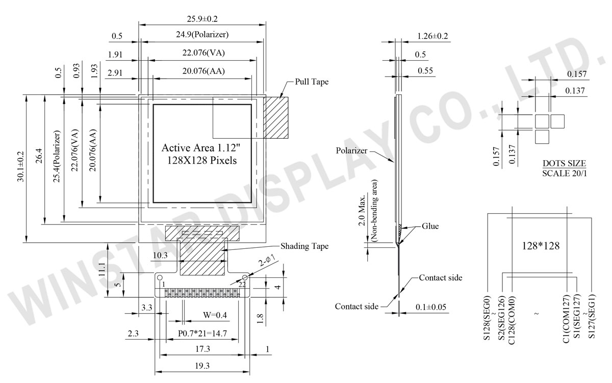
WEO128128Gは1.12インチホットバーFPC付きのCOG構造のグラフィック有機ELディスプレイで、解像度は128x128です。SH1107 ICを内蔵し、6800/8080 8ビット パラレル、4線式のSPI、 I2Cインターフェイスをサポート致します。ロジックの電源電圧は3V (標準値) で、ディスプレイの電源電圧は12Vで、50%チェックボード電流での表示は15mA @ VCC 12V (白色の発光色)で、駆動デューティは1/128です。
WEO128128Gは超薄、軽量、低消費電力のメリットがあり、メーター、スマートホームアプリケーション、ポストシステム、Cloud/IoTシステム、ハンドヘルド機器、インテリジェントテクノロジーデバイス、エネルギーシステム、自動車用、通信システム、医療機器などに適しております。 操作温度範囲は-40℃~ +80℃で、保存温度範囲は-40℃~ +85℃です。
| 項目 | 仕様 | 単位 |
|---|---|---|
| ドットマトリックス(解像度) | 128 × 128 | - |
| モジュールサイズ | 25.9 x 30.1 x 1.26 | mm |
| 有効エリア | 20.076 x 20.076 | mm |
| ドットサイズ | 0.137 x 0.137 | mm |
| ドットピッチ | 0.157 x 0.157 | mm |
| 表示モード | パッシブマトリックス | |
| 発光色 | モノクロ | |
| 駆動方法 | 1/128 Duty | |
| IC | SH1107 | |
| インターフェイス | 6800,8080,4-wire SPI,I2C | |
| 表示サイズ(対角線) | 1.12 インチ | |
| パラメーター | 記号 | 最小値 | 最大値 | 単位 |
|---|---|---|---|---|
| ロジック電源電圧 | VDD | -0.3 | 3.6 | V |
| Display電源電圧 | VPP | -0.3 | 17.0 | V |
| 操作温度 | TOP | -40 | +80 | °C |
| 保存温度 | TSTG | -40 | +85 | °C |
| 項目 | 記号 | 条件 | 最小値 | 典型値 | 最大値 | 単位 |
|---|---|---|---|---|---|---|
| ロジック電源電圧 | VDD | - | 1.65 | 3.0 | 3.3 | V |
| Display電源電圧 | VPP | - | 7.0 | 12.0 | 12.5 | V |
| 高レベル入力電圧 | VIH | - | 0.8×VDD | - | VDD | V |
| 低レベル入力電圧 | VIL | - | 0 | - | 0.2×VDD | V |
| 高レベル出力電圧 | VOH | - | 0.8×VDD | - | VDD | V |
| 低レベル出力電圧 | VOL | - | 0 | - | 0.2×VDD | V |
| 50% Check Board operating Current | IPP | VPP=12V | - | 15.0 | 25.0 | mA |
| No. | 記号 | 説明 | |||||||||||||||
|---|---|---|---|---|---|---|---|---|---|---|---|---|---|---|---|---|---|
| 1 | VPP | This is the most positive voltage supply pad of the chip. It should be supplied externally. |
|||||||||||||||
| 2 | VCOMH | This is a pad for the voltage output high level for common signals. A capacitor should be connected between this pad and VSS. |
|||||||||||||||
| 3 | VDD | Power supply for logic and input. | |||||||||||||||
| 4 | NC | Not connected. | |||||||||||||||
| 5 | IM1 | These are the MPU interface mode select pads.
|
|||||||||||||||
| 6 | IM2 | ||||||||||||||||
| 7 | IREF | This is a segment current reference pad. A resistor should be connected between this pad and VSS. Set the current at 15.625uA. | |||||||||||||||
| 8 | CS | This pad is the chip select input. When CS = “L”, then the chip select becomes active, and data/command I/O is enabled. | |||||||||||||||
| 9 | RES | This is a reset signal input pad. When RES is set to “L”, the settings are initialized. The reset operation is performed by the RES signal level. | |||||||||||||||
| 10 | A0 | This is the Data/Command control pad that determines whether the data bits are data or a command. A0 = “H”: the inputs at D0 to D7 are treated as display data. A0 = “L”: the inputs at D0 to D7 are transferred to the command registers. In I2C interface, this pad serves as SA0 to distinguish the different address of OLED driver. |
|||||||||||||||
| 11 | WR | This is a MPU interface input pad. When connected to an 8080 MPU, this is active LOW. This pad connects to the 8080 MPU WR signal. The signals on the data bus are latched at the rising edge of the WR signal. When connected to a 6800 Series MPU: This is the read/write control signal input terminal. When WR = “H”: Read. When WR = “L”: Write. |
|||||||||||||||
| 12 | E/RD | This is a MPU interface input pad. When connected to an 8080 series MPU, it is active LOW. This pad is connected to the RD signal of the 8080 series MPU, and the data bus is in an output status when this signal is “L”. When connected to a 6800 series MPU, this is active HIGH. This is used as an enable clock input of the 6800 series MPU. |
|||||||||||||||
| 13~20 | D0~D7 | This is an 8-bit bi-directional data bus that connects to an 8-bit or 16-bit standard MPU data bus. When the serial interface is selected, then D0 serves as the serial clock input pad (SCL) and D1serves as the serial data input pad (SI). At this time, D2 to D7 are set to high impedance. When the I2C interface is selected, then D0 serves as the serial clock input pad (SCL) and D1 serves as the serial data input pad (SDA). At this time, D2 to D7 are set to high impedance. |
|||||||||||||||
| 21 | GND | Ground | |||||||||||||||
| 22 | NC | Not connected. |

「すべてのクッキーを許可」をクリックすると、サイトのナビゲーションを向上させ、サイト使用状況を分析し、マーケティングおよびパフォーマンスの取り組みを支援するために、クッキーをデバイスに保存することに同意したことになります。この件に関する詳細情報は、ポリシーをご覧ください。プライバシーポリシー