
 - WEO025664D-CTP")
私たちはあなたのプライバシーを大切にします
「すべてのクッキーを許可」をクリックすると、サイトのナビゲーションを向上させ、サイト使用状況を分析し、マーケティングおよびパフォーマンスの取り組みを支援するために、クッキーをデバイスに保存することに同意したことになります。この件に関する詳細情報は、ポリシーをご覧ください。プライバシーポリシー


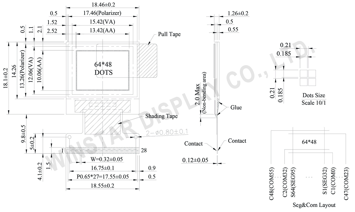
WEO006448Aは0.66インチ、64×48ピクセルの単色OLEDディスプレイモジュールです。外形寸法は18.46×18.10×1.26 mm、AAサイズは13.42×10.06 mmです。SSD1306 ICを内蔵し、6800/8080 8ビットパラレル、I2C、4線シリアルインターフェースに対応しています。
このOLEDモジュールはCOG構造で厚さ1.26mm、軽量かつ低消費電力です。動作温度範囲は-40℃~+80℃、保存温度範囲は-40℃~+80℃です。内部チャージポンプおよび外部VCC電源に対応しています。ウェアラブル機器、MP3、携帯機器、パーソナルケア機器、ボイスレコーダー、健康機器などに利用可能です。

Data source ref: WEO006448AWPP3N00000
| 項目 | 仕様 | 単位 |
|---|---|---|
| ドットマトリックス | 64 x 48 Dots | - |
| モジュールサイズ | 18.46 × 18.10 × 1.26 | mm |
| アクティブエリア | 13.42 × 10.06 | mm |
| ピクセルサイズ | 0.185 × 0.185 | mm |
| ピクセルピッチ | 0.210 × 0.210 | mm |
| 表示モード | パッシブマトリクス(Passive Matrix) | |
| 表示カラー | モノクロ | |
| 駆動方法 | 1/48 Duty | |
| IC | SSD1306 | |
| インターフェイス | 6800, 8080, 4-Wire SPI, I2C | |
| 表示サイズ(対角線) | 0.66 インチ | |
| パラメーター | 記号 | 最小値 | 最大値 | 単位 |
|---|---|---|---|---|
| ロジック電源電圧 | VDD | 0 | 4.0 | V |
| 表示用電源電圧 | VCC | 0 | 15.0 | V |
| 操作温度 | TOP | -40 | +80 | °C |
| 保存温度 | TSTG | -40 | +85 | °C |
| 項目 | 記号 | 条件 | 最小値 | 典型値 | 最大値 | 単位 |
|---|---|---|---|---|---|---|
| ロジック電源電圧 | VDD | - | 1.65 | 3.0 | 3.3 | V |
| ディスプレイの供給電圧(外部供給) | VCC | - | 6.0 | 7.5 | 8.0 | V |
| チャージポンプレギュレータ供給電圧 | VBAT | - | 3.0 | - | 4.2 | V |
| チャージポンプ出力電圧(内部DC/DC生成) | Charge Pump VCC |
- | 7.0 | 7.5 | - | V |
| 高レベル入力電圧 | VIH | - | 0.8×VDD | - | VDD | V |
| 低レベル入力電圧 | VIL | - | 0 | - | 0.2×VDD | V |
| 高レベル出力電圧 | VOH | - | 0.9×VDD | - | VDD | V |
| 低レベル出力電圧 | VOL | - | 0 | - | 0.1×VDD | V |
| ディスプレイ50%ピクセル点灯(VCC外部供給) | ICC | VCC=7.5V | - | 6 | 13 | mA |
| ディスプレイ50%ピクセル点灯(VCC内部DC/DC生成) | IBAT | - | - | 15 | 23 | mA |
| No. | 記号 | 説明 | |||||||||||||||
|---|---|---|---|---|---|---|---|---|---|---|---|---|---|---|---|---|---|
| 1 | ESD-GND | It should be connected to ground. | |||||||||||||||
| 2 | C2N | C1P/C1N – Pin for charge pump capacitor; Connect to each other with a capacitor. C2P/C2N – Pin for charge pump capacitor; Connect to each other with a capacitor. |
|||||||||||||||
| 3 | C2P | ||||||||||||||||
| 4 | C1P | ||||||||||||||||
| 5 | C1N | ||||||||||||||||
| 6 | VBAT | This is the power supply pin for the internal buffer of the DC/DC voltage converter. It must be connected to external source when the converter is used. It should be connected to VDD or kept float when the converter is not used. | |||||||||||||||
| 7 | VSS | This is a ground pin. | |||||||||||||||
| 8 | VDD | Power supply pin for core logic operation. | |||||||||||||||
| 9 | BS1 | These pins are MCU interface selection input. See the following table:
|
|||||||||||||||
| 10 | BS2 | ||||||||||||||||
| 11 | CS# | This pin is the chip select input. (active LOW). | |||||||||||||||
| 12 | RES# | This pin is reset signal input. When the pin is low, initialization of the chip is executed. Keep this pin HIGH (i.e. connect to VDD) during normal operation. | |||||||||||||||
| 13 | D/C# | This is Data/Command control pin. When it is pulled HIGH (i.e. connect to VDD), the data at D[7:0] is treated as data. When it is pulled LOW, the data at D[7:0] will be transferred to the command register. In I2C mode, this pin acts as SA0 for slave address selection. |
|||||||||||||||
| 14 | R/W# | This is read / write control input pin connecting to the MCU interface. When interfacing to a 6800-series microprocessor, this pin will be used as Read/Write (R/W#) selection input. Read mode will be carried out when this pin is pulled HIGH (i.e. connect to VDD) and write mode when LOW. When 8080 interface mode is selected, this pin will be the Write (WR#) input. Data write operation is initiated when this pin is pulled LOW and the chip is selected. When serial or I2C interface is selected, this pin must be connected to VSS. |
|||||||||||||||
| 15 | E/RD# | When interfacing to a 6800-series microprocessor, this pin will be used as the Enable (E) signal. Read/write operation is initiated when this pin is pulled HIGH (i.e. connect to VDD) and the chip is selected. When connecting to an 8080-series microprocessor, this pin receives the Read (RD#) signal. Read operation is initiated when this pin is pulled LOW and the chip is selected. When serial or I2C interface is selected, this pin must be connected to VSS |
|||||||||||||||
| 16~23 | D0~D7 | These are 8-bit bi-directional data bus to be connected to the microprocessor’s data bus. When serial interface mode is selected, D0 will be the serial clock input: SCLK; D1 will be the serial data input: SDIN. When I2C mode is selected, D2, D1 should be tied together and serve as SDAout, SDAin in application and D0 is the serial clock input, SCL. |
|||||||||||||||
| 24 | IREF | This is segment output current reference pin. When external IREF is used, a resistor should be connected between this pin and VSS to maintain the IREF current at a maximum of 30uA.When internal IREF is used, this pin should be kept NC. |
|||||||||||||||
| 25 | VCOMH | The pin for COM signal deselected voltage level. A capacitor should be connected between this pin and VSS. | |||||||||||||||
| 26 | VCC | Power supply for panel driving voltage. This is also the most positive power voltage supply pin. When charge pump is enabled, a capacitor should be connected between this pin and VSS. |
|||||||||||||||
| 27 | VLSS | This is an analog ground pin. It should be connected to VSS externally. | |||||||||||||||
| 28 | ESD GND | It should be connected to ground. |

「すべてのクッキーを許可」をクリックすると、サイトのナビゲーションを向上させ、サイト使用状況を分析し、マーケティングおよびパフォーマンスの取り組みを支援するために、クッキーをデバイスに保存することに同意したことになります。この件に関する詳細情報は、ポリシーをご覧ください。プライバシーポリシー