
私たちはあなたのプライバシーを大切にします
「すべてのクッキーを許可」をクリックすると、サイトのナビゲーションを向上させ、サイト使用状況を分析し、マーケティングおよびパフォーマンスの取り組みを支援するために、クッキーをデバイスに保存することに同意したことになります。この件に関する詳細情報は、ポリシーをご覧ください。プライバシーポリシー


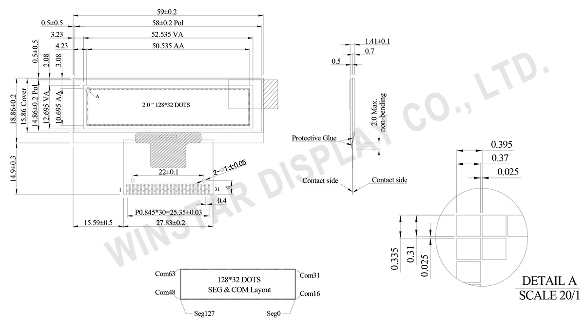
WEO012832Kは解像度128x32ドットの2.0インチのホットバーFPCを備えたCOG構造で、グラフィックOLEDディスプレイです。このモジュールはSSD1315 ICに内蔵されて、6800/8080・8ビットパラレルで、I2C及び4-Wire SPIインタフェースを使用できて、ロジック3Vの電源電圧にして、1/32デューティサイクル にします。内部チャージポンプ電源と外部 VCC 電源をサポートしております。
WE012832KはICが廃止されたことで生産停止されているTAB OLED WEX012832Aのピンと互換性が有って、 顧客がハードウェアを変更する必要は有りませんが、初期コードを変更する必要になります。このモジュールは産業機器、スマートホームアプリケーション、医療機器等に適して、操作温度範囲が40℃〜 80℃で、保存温度範囲が-40℃〜 85℃です。
Data source ref: WEO012832KWPP3N00000
| 項目 | 仕様 | 単位 |
|---|---|---|
| ドットマトリックス(解像度) | 128 x 32 | Dots |
| 外形寸法 | 59.0 × 18.86 × 1.41 | mm |
| 有効表示エリア | 50.535 × 10.695 | mm |
| ドットサイズ | 0.370 × 0.310 | mm |
| ドットピッチ | 0.395 × 0.335 | mm |
| 表示モード | パッシブマトリクス | |
| 発光色 | モノクロ | |
| インターフェイス | 8Bits 6800 8080/ 4-Wire SPI/ I2C | |
| 駆動方法 | 1/32 Duty | |
| IC | SSD1315 | |
| サイズ | 2 インチ | |
| パラメーター | 記号 | 最小値 | 典型値 | 最大値 | 単位 |
|---|---|---|---|---|---|
| ロジック電源電圧 | VDD | -0.3 | - | 4 | V |
| Display電源電圧 | VCC | 0 | - | 18 | V |
| 操作温度 | TOP | -40 | - | 80 | °C |
| 保存温度 | TSTG | -40 | - | 85 | °C |
| 項目 | 記号 | 最小値 | 典型値 | 最大値 | 単位 | |
|---|---|---|---|---|---|---|
| Supply Voltage | ロジック | VDD | 2.8 | 3.0 | 3.3 | V |
| 動作 | VCC | 7.5 | 8.0 | 8.5 | V | |
| 入力電圧 | 高電圧 | VIH | 0.8 x VDD | - | VDD | V |
| 低電圧 | VIL | 0 | - | 0.2 x VDD | V | |
| 出力電圧 | 高電圧 | VOH | 0.9x VDD | - | VDD | V |
| 低電圧 | VOL | 0 | - | 0.1 x VDD | V | |
| 記号 | パラメーター | 最小値 | 典型値 | 最大値 | 単位 | 条件 |
|---|---|---|---|---|---|---|
| ICC | VCC Supply Current | - | 11 | 22 | mA | VDD=3V , VCC=8.0, Display 50% ON |
| No. | 記号 | 説明 |
|---|---|---|
| 1 | NC | No connection |
| 2 | VCC | Power supply for panel driving voltage. This is also the most positive power voltage supply pin. When charge pump is enabled, a capacitor should be connected between this pin and VSS. |
| 3 | VCOMH | COM signal deselected voltage level. A capacitor should be connected between this pin and VSS. |
| 4 | IREF | This is segment output current reference pin. When external IREF is used, a resistor should be connected between this pin and VSS to maintain the IREF current at 30uA. |
| 5 | D7 | These are 8-bit bi-directional data bus to be connected to the microprocessor’s data bus. When serial interface mode is selected, D0 will be the serial clock input: SCLK; D1 will be the serial data input: SDIN. When I2C mode is selected, D2, D1 should be tied together and serve as SDAout, SDAin in application and D0 is the serial clock input, SCL. |
| 6 | D6 | |
| 7 | D5 | |
| 8 | D4 | |
| 9 | D3 | |
| 10 | D2 | |
| 11 | D1 | |
| 12 | D0 | |
| 13 | E/RD# | This pin is MCU interface input. When 6800 interface mode is selected, this pin will be used as the Enable (E) signal. Read/write operation is initiated when this pin is pulled HIGH and the chip is selected. When 8080 interface mode is selected, this pin receives the Read (RD#) signal. Read operation is initiated when this pin is pulled LOW and the chip is selected. When serial or I2C interface is selected, this pin must be connected to VSS. |
| 14 | R/W# | This is read / write control input pin connecting to the MCU interface. When interfacing to a 6800-series microprocessor, this pin will be used as Read/Write (R/W#) selection input. Read mode will be carried out when this pin is pulled HIGH (i.e. connect to VDD) and write mode when LOW. When 8080 interface mode is selected, this pin will be the Write (WR#) input. Data write operation is initiated when this pin is pulled LOW and the chip is selected. When serial or I2C interface is selected, this pin must be connected to VSS. |
| 15 | D/C# | This pin is Data/Command control pin connecting to the MCU. When the pin is pulled HIGH, the data at D[7:0] will be interpreted as data. When the pin is pulled LOW, the data at D[7:0] will be transferred to a command register. |
| 16 | RES# | This pin is reset signal input. When the pin is pulled LOW, initialization of the chip is executed. Keep this pin HIGH (i.e. connect to VDD) during normal operation. |
| 17 | CS# | This pin is the chip select input connecting to the MCU. The chip is enabled for MCU communication only when CS# is pulled LOW (active LOW). |
| 18 | NC | No connection |
| 19 | BS2 | MCU bus interface selection pins. Select appropriate logic setting as described in the following table. BS2, BS1 are pin select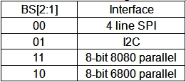 Note (1) 0 is connected to VSS (2) 1 is connected to VDD |
| 20 | BS1 | |
| 21 | VDD | Power supply pin for core logic operation. This is a voltage supply pin. It must be connected to external source. |
| 22~29 | NC | No connection |
| 30 | VSS | Ground pin. It must be connected to external ground. |
| 31 | NC | No connection |

「すべてのクッキーを許可」をクリックすると、サイトのナビゲーションを向上させ、サイト使用状況を分析し、マーケティングおよびパフォーマンスの取り組みを支援するために、クッキーをデバイスに保存することに同意したことになります。この件に関する詳細情報は、ポリシーをご覧ください。プライバシーポリシー