

 配备铁框 - WEF012864U")
我们重视您的隐私
通过点击「允许所有 Cookie」,代表您同意在您的设备上存储 Cookie 以增强网站浏览体验、分析网站使用情况并协助我们的营销和网站效能优化工作。您可以在我们的隐私权政策中找到有关于此的更多信息。


华凌「超薄微小型OLED显示屏」WEO006448A是一款0.66寸小尺寸单色被动式OLED显示器模块,分辨率为64 x 48 点阵组成。WEO006448A模块尺寸为18.46 × 18.10 × 1.26 mm, AA区尺寸为13.42 × 10.06 mm。WEO006448A内置SSD1306 控制器, 模块支持多种传输接口: 6800 8-bite, 8080 8-bit 并行接口, I2C与4线SPI串行接口,使用3V电压驱动。此模块的工作温度是-40℃至+80℃,储存温度-40℃至+80℃。此型号OLED模块可支持内部升压及外部供电。
OLED优异高质感显示效果,产品自发光无须背光源,重量轻且低耗电,适用穿戴装置、智能产品、手持式量测仪器、医疗仪器和工业控制设备等,产品特色:

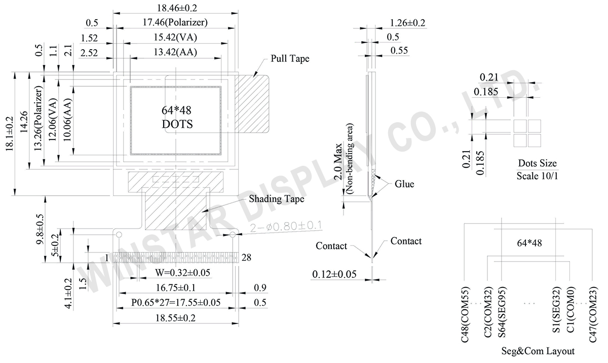
Data source ref: WEO006448AWPP3N00000
| 项目 | 尺寸 | 单位 |
|---|---|---|
| 点阵 | 64 x 48 Dots | - |
| 模块尺寸 | 18.46 × 18.10 × 1.26 | mm |
| 有效区域 | 13.42 × 10.06 | mm |
| 像素大小 | 0.185 × 0.185 | mm |
| 像素间距 | 0.210 × 0.210 | mm |
| 显示模式 | 被动矩阵(Passive Matrix) | |
| 显示颜色 | 单色 | |
| 驱动方式 | 1/48 Duty | |
| IC | SSD1306 | |
| 接口 | 6800, 8080, 4-Wire SPI, I2C | |
| 对角线尺寸 | 0.66 寸 | |
| 参数 | 符号 | 最小值 | 最大值 | 单位 |
|---|---|---|---|---|
| 逻辑电源电压 | VDD | 0 | 4.0 | V |
| 显示电源电压 | VCC | 0 | 15.0 | V |
| 工作温度 | TOP | -40 | +80 | °C |
| 储存温度 | TSTG | -40 | +85 | °C |
| 项目 | 符号 | 条件 | 最小值 | 典型值 | 最大值 | 单位 |
|---|---|---|---|---|---|---|
| 逻辑电源电压 | VDD | - | 1.65 | 3.0 | 3.3 | V |
| 显示器供电电压(外部供应) | VCC | - | 6.0 | 7.5 | 8.0 | V |
| 电荷帮浦稳压器电源电压 | VBAT | - | 3.0 | - | 4.2 | V |
| 显示器的电荷帮浦输出电压(由内部DC/DC生成) | Charge Pump VCC |
- | 7.0 | 7.5 | - | V |
| 输入高电压 | VIH | - | 0.8×VDD | - | VDD | V |
| 输入低电压 | VIL | - | 0 | - | 0.2×VDD | V |
| 输出高电压 | VOH | - | 0.9×VDD | - | VDD | V |
| 输出低电压 | VOL | - | 0 | - | 0.1×VDD | V |
| 显示器 50% 像素开启(VCC 由外部供应) | ICC | VCC=7.5V | - | 6 | 13 | mA |
| 显示器 50% 像素开启(VCC 由内部 DC/DC 生成) | IBAT | - | - | 15 | 23 | mA |
| No. | 符号 | 功能说明 | |||||||||||||||
|---|---|---|---|---|---|---|---|---|---|---|---|---|---|---|---|---|---|
| 1 | ESD-GND | It should be connected to ground. | |||||||||||||||
| 2 | C2N | C1P/C1N – Pin for charge pump capacitor; Connect to each other with a capacitor. C2P/C2N – Pin for charge pump capacitor; Connect to each other with a capacitor. |
|||||||||||||||
| 3 | C2P | ||||||||||||||||
| 4 | C1P | ||||||||||||||||
| 5 | C1N | ||||||||||||||||
| 6 | VBAT | This is the power supply pin for the internal buffer of the DC/DC voltage converter. It must be connected to external source when the converter is used. It should be connected to VDD or kept float when the converter is not used. | |||||||||||||||
| 7 | VSS | This is a ground pin. | |||||||||||||||
| 8 | VDD | Power supply pin for core logic operation. | |||||||||||||||
| 9 | BS1 | These pins are MCU interface selection input. See the following table:
|
|||||||||||||||
| 10 | BS2 | ||||||||||||||||
| 11 | CS# | This pin is the chip select input. (active LOW). | |||||||||||||||
| 12 | RES# | This pin is reset signal input. When the pin is low, initialization of the chip is executed. Keep this pin HIGH (i.e. connect to VDD) during normal operation. | |||||||||||||||
| 13 | D/C# | This is Data/Command control pin. When it is pulled HIGH (i.e. connect to VDD), the data at D[7:0] is treated as data. When it is pulled LOW, the data at D[7:0] will be transferred to the command register. In I2C mode, this pin acts as SA0 for slave address selection. |
|||||||||||||||
| 14 | R/W# | This is read / write control input pin connecting to the MCU interface. When interfacing to a 6800-series microprocessor, this pin will be used as Read/Write (R/W#) selection input. Read mode will be carried out when this pin is pulled HIGH (i.e. connect to VDD) and write mode when LOW. When 8080 interface mode is selected, this pin will be the Write (WR#) input. Data write operation is initiated when this pin is pulled LOW and the chip is selected. When serial or I2C interface is selected, this pin must be connected to VSS. |
|||||||||||||||
| 15 | E/RD# | When interfacing to a 6800-series microprocessor, this pin will be used as the Enable (E) signal. Read/write operation is initiated when this pin is pulled HIGH (i.e. connect to VDD) and the chip is selected. When connecting to an 8080-series microprocessor, this pin receives the Read (RD#) signal. Read operation is initiated when this pin is pulled LOW and the chip is selected. When serial or I2C interface is selected, this pin must be connected to VSS |
|||||||||||||||
| 16~23 | D0~D7 | These are 8-bit bi-directional data bus to be connected to the microprocessor’s data bus. When serial interface mode is selected, D0 will be the serial clock input: SCLK; D1 will be the serial data input: SDIN. When I2C mode is selected, D2, D1 should be tied together and serve as SDAout, SDAin in application and D0 is the serial clock input, SCL. |
|||||||||||||||
| 24 | IREF | This is segment output current reference pin. When external IREF is used, a resistor should be connected between this pin and VSS to maintain the IREF current at a maximum of 30uA.When internal IREF is used, this pin should be kept NC. |
|||||||||||||||
| 25 | VCOMH | The pin for COM signal deselected voltage level. A capacitor should be connected between this pin and VSS. | |||||||||||||||
| 26 | VCC | Power supply for panel driving voltage. This is also the most positive power voltage supply pin. When charge pump is enabled, a capacitor should be connected between this pin and VSS. |
|||||||||||||||
| 27 | VLSS | This is an analog ground pin. It should be connected to VSS externally. | |||||||||||||||
| 28 | ESD GND | It should be connected to ground. |

通过点击「允许所有 Cookie」,代表您同意在您的设备上存储 Cookie 以增强网站浏览体验、分析网站使用情况并协助我们的营销和网站效能优化工作。您可以在我们的隐私权政策中找到有关于此的更多信息。