
우리는 귀하의 프라이버시를 소중히 여깁니다
"모든 쿠키 허용"을 클릭하면 사이트 탐색을 개선하고, 사이트 사용을 분석하며, 마케팅 및 성능 노력에 도움을 주기 위해 쿠키를 귀하의 장치에 저장하는 데 동의한 것으로 간주됩니다. 이 주제에 대한 추가 정보는 당사의 정책에서 확인할 수 있습니다. 개인정보 보호정책


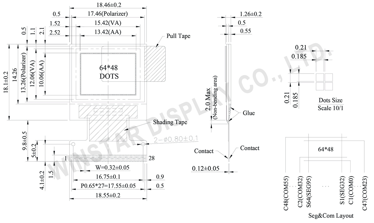
WINSTAR WEO006448A는 64x48 픽셀로 구성된 미니 OLED 디스플레이로, 대각선 크기는 0.66인치에 불과합니다. WEO006448A는 18.46 × 18.10 × 1.26 mm의 외형 크기와 13.42 × 10.06 mm의 활성 영역(AA) 크기를 가지고 있습니다. 내장된 SSD1306 컨트롤러 IC는 6800/8080 8비트 병렬, I2C 및 4-wire 직렬 인터페이스를 통해 통신할 수 있습니다. WEO006448A 모듈은 내부 차지 펌프 전원 공급과 외부 VCC 전원 공급을 모두 지원합니다. 이 디스플레이는 초박형(두께 1.3mm), 가벼운 무게와 저전력 소비를 자랑하는 COG OLED 디스플레이입니다. 웨어러블 기기, MP3 플레이어, 휴대용 장치, 개인 관리 기기, 음성 녹음기, 헬스케어 기기 등 다양한 분야에 적합합니다.
WEO006448A 미니 OLED 디스플레이 모듈은 -40°C에서 +80°C까지의 온도 범위에서 작동하며, 보관 온도는 -40°C에서 +80°C까지 지원됩니다. 아래는 WEO006448A의 기본 사양입니다. 샘플이나 견적에 대한 자세한 내용은 공식 웹사이트의 '문의하기' 페이지를 통해 문의해 주세요.

Data source ref: WEO006448AWPP3N00000
| 항목 | 치수 | 단위 |
|---|---|---|
| 도트 매트릭스 | 64 x 48 Dots | - |
| 모듈 치수 | 18.46 × 18.10 × 1.26 | mm |
| 활성 영역 | 13.42 × 10.06 | mm |
| 픽셀 크기 | 0.185 × 0.185 | mm |
| 픽셀 피치 | 0.210 × 0.210 | mm |
| 디스플레이 모드 | 패시브 매트릭스 (Passive Matrix) | |
| 디스플레이 색상 | 단색 | |
| 구동 듀티 | 1/48 Duty | |
| IC | SSD1306 | |
| 인터페이스 | 6800, 8080, 4-Wire SPI, I2C | |
| 크기 (대각선) | 0.66 인치 | |
| 매개변수 | 기호 | 최소값 | 최대값 | 단위 |
|---|---|---|---|---|
| 논리 회로 공급 전압 | VDD | 0 | 4.0 | V |
| 디스플레이 전원 공급 전압 | VCC | 0 | 15.0 | V |
| 작동 온도 | TOP | -40 | +80 | °C |
| 보관 온도 | TSTG | -40 | +85 | °C |
| 항목 | 기호 | 조건 | 최소값 | 대표값 | 최대값 | 단위 |
|---|---|---|---|---|---|---|
| 논리용 전원 공급 전압 | VDD | - | 1.65 | 3.0 | 3.3 | V |
| 디스플레이 전원 공급 전압 (외부 공급) | VCC | - | 6.0 | 7.5 | 8.0 | V |
| 차지 펌프 레귤레이터 전원 공급 전압 | VBAT | - | 3.0 | - | 4.2 | V |
| 디스플레이 차지 펌프 출력 전압 (내부 DC/DC 생성) | Charge Pump VCC |
- | 7.0 | 7.5 | - | V |
| 입력 고전압 | VIH | - | 0.8×VDD | - | VDD | V |
| 입력 저전압 | VIL | - | 0 | - | 0.2×VDD | V |
| 출력 고전압 | VOH | - | 0.9×VDD | - | VDD | V |
| 출력 저전압 | VOL | - | 0 | - | 0.1×VDD | V |
| 디스플레이 50% 픽셀 켜짐 (VCC 외부 공급) | ICC | VCC=7.5V | - | 6 | 13 | mA |
| 디스플레이 50% 픽셀 켜짐 (VCC 내부 DC/DC 생성) | IBAT | - | - | 15 | 23 | mA |
| No. | 기호 | 기능 | |||||||||||||||
|---|---|---|---|---|---|---|---|---|---|---|---|---|---|---|---|---|---|
| 1 | ESD-GND | It should be connected to ground. | |||||||||||||||
| 2 | C2N | C1P/C1N – Pin for charge pump capacitor; Connect to each other with a capacitor. C2P/C2N – Pin for charge pump capacitor; Connect to each other with a capacitor. |
|||||||||||||||
| 3 | C2P | ||||||||||||||||
| 4 | C1P | ||||||||||||||||
| 5 | C1N | ||||||||||||||||
| 6 | VBAT | This is the power supply pin for the internal buffer of the DC/DC voltage converter. It must be connected to external source when the converter is used. It should be connected to VDD or kept float when the converter is not used. | |||||||||||||||
| 7 | VSS | This is a ground pin. | |||||||||||||||
| 8 | VDD | Power supply pin for core logic operation. | |||||||||||||||
| 9 | BS1 | These pins are MCU interface selection input. See the following table:
|
|||||||||||||||
| 10 | BS2 | ||||||||||||||||
| 11 | CS# | This pin is the chip select input. (active LOW). | |||||||||||||||
| 12 | RES# | This pin is reset signal input. When the pin is low, initialization of the chip is executed. Keep this pin HIGH (i.e. connect to VDD) during normal operation. | |||||||||||||||
| 13 | D/C# | This is Data/Command control pin. When it is pulled HIGH (i.e. connect to VDD), the data at D[7:0] is treated as data. When it is pulled LOW, the data at D[7:0] will be transferred to the command register. In I2C mode, this pin acts as SA0 for slave address selection. |
|||||||||||||||
| 14 | R/W# | This is read / write control input pin connecting to the MCU interface. When interfacing to a 6800-series microprocessor, this pin will be used as Read/Write (R/W#) selection input. Read mode will be carried out when this pin is pulled HIGH (i.e. connect to VDD) and write mode when LOW. When 8080 interface mode is selected, this pin will be the Write (WR#) input. Data write operation is initiated when this pin is pulled LOW and the chip is selected. When serial or I2C interface is selected, this pin must be connected to VSS. |
|||||||||||||||
| 15 | E/RD# | When interfacing to a 6800-series microprocessor, this pin will be used as the Enable (E) signal. Read/write operation is initiated when this pin is pulled HIGH (i.e. connect to VDD) and the chip is selected. When connecting to an 8080-series microprocessor, this pin receives the Read (RD#) signal. Read operation is initiated when this pin is pulled LOW and the chip is selected. When serial or I2C interface is selected, this pin must be connected to VSS |
|||||||||||||||
| 16~23 | D0~D7 | These are 8-bit bi-directional data bus to be connected to the microprocessor’s data bus. When serial interface mode is selected, D0 will be the serial clock input: SCLK; D1 will be the serial data input: SDIN. When I2C mode is selected, D2, D1 should be tied together and serve as SDAout, SDAin in application and D0 is the serial clock input, SCL. |
|||||||||||||||
| 24 | IREF | This is segment output current reference pin. When external IREF is used, a resistor should be connected between this pin and VSS to maintain the IREF current at a maximum of 30uA.When internal IREF is used, this pin should be kept NC. |
|||||||||||||||
| 25 | VCOMH | The pin for COM signal deselected voltage level. A capacitor should be connected between this pin and VSS. | |||||||||||||||
| 26 | VCC | Power supply for panel driving voltage. This is also the most positive power voltage supply pin. When charge pump is enabled, a capacitor should be connected between this pin and VSS. |
|||||||||||||||
| 27 | VLSS | This is an analog ground pin. It should be connected to VSS externally. | |||||||||||||||
| 28 | ESD GND | It should be connected to ground. |

"모든 쿠키 허용"을 클릭하면 사이트 탐색을 개선하고, 사이트 사용을 분석하며, 마케팅 및 성능 노력에 도움을 주기 위해 쿠키를 귀하의 장치에 저장하는 데 동의한 것으로 간주됩니다. 이 주제에 대한 추가 정보는 당사의 정책에서 확인할 수 있습니다. 개인정보 보호정책