
我們重視您的隱私
通過點擊「允許所有 Cookie」,代表您同意在您的設備上存儲 Cookie 以增強網站瀏覽體驗、分析網站使用情況並協助我們的行銷和網站效能優化工作。您可以在我們的隱私權政策中找到有關於此的更多資訊。

 - WEO020636A")
 - WEO020636A")
 - WEO020636A")
 - WEO020636A")
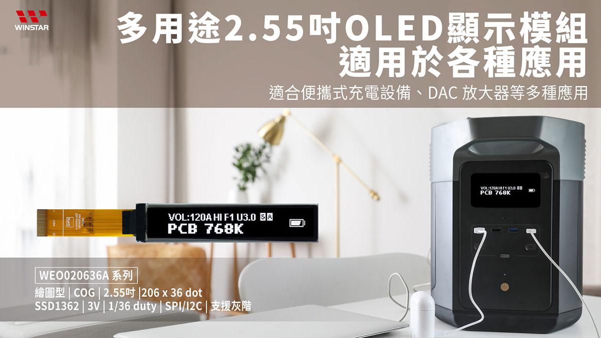
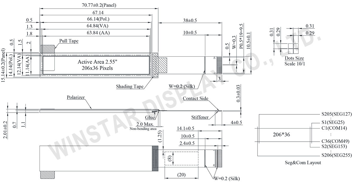
WEO020636A 系列是華凌首次發表的規格 2.55 吋 OLED 顯示模組,解析度為 206x36 dots。這款 COG(Chip on Glass)繪圖型 OLED 顯示器的外形尺寸為 70.77 x 15.14 mm,有效顯示區域為 63.84 x 11.14 mm,提供精確的視覺表現。
WEO020636A OLED 顯示器非常適合於多種應用,包括隨身型 DAC (Digital-to-Analog Converter) 耳擴、便攜式充電設備、小型音響。其纖薄的尺寸和出色的視覺清晰度,使其適用於手持裝置、工業設備、醫療設備和消費電子產品。該顯示器的 COG 結構及其對 SPI 和 I2C 介面的相容性,能夠無縫整合到各種數位環境中。
增強視覺表現:無論是在手持裝置中增強用戶介面,還是在工業設置中提供重要的視覺反饋,WEO020636A 都能在廣泛的溫度範圍內保證可靠的性能和耐用性。
| 項目 | 標準尺寸 | 單位 |
|---|---|---|
| 點陣(解析度) | 206 x 36 Dots | - |
| 模組尺寸 | 70.77 x 15.14 x 2.01 | mm |
| 有效區域 | 63.84 x 11.14 | mm |
| 點大小 | 0.29 x 0.29 | mm |
| 點間距 | 0.31 x 0.31 | mm |
| 顯示模式 | 被動矩陣 | |
| 發光顏色 | 單色 | |
| 驅動方式 | 1/36 Duty | |
| 灰階 | 4 Bits | |
| IC | SSD1362 | |
| 介面 | 3-Wire SPI、4-Wire SPI、I2C | |
| 顯示尺寸(對角線) | 2.55 inch | |
| 參數 | 符號 | 最小值 | 最大值 | 單位 |
|---|---|---|---|---|
| 供電電壓 | VDD | -0.5 | 2.75 | V |
| 供電電壓 | VCI | -0.3 | 5.5 | V |
| 供電電壓 | VDDIO | -0.5 | 5.5 | V |
| 供電電壓 | VCC | 7 | 21 | V |
| 工作溫度 | TOP | -40 | +80 | °C |
| 儲存溫度 | TSTG | -40 | +85 | °C |
| 項目 | 符號 | 條件 | 最小值 | 典型值 | 最大值 | 單位 |
|---|---|---|---|---|---|---|
| 顯示電壓 | VCC | - | 10.0 | 12.0 | 12.5 | V |
| 低電壓電源 | VCI | - | 1.65 | - | 3.5 | V |
| I/O pins 電源 | VDDIO | - | 1.65 | - | VCI | V |
| 邏輯電源電壓 | VDD | - | 1.65 | - | 2.6 | V |
| 輸入高電壓 | VIH | - | 0.8×VDDIO | - | - | V |
| 輸入低電壓 | VIL | - | - | - | 0.2×VDDIO | V |
| 輸出高電壓 | VOH | - | 0.9×VDDIO | - | - | V |
| 輸出低電壓 | VOL | - | - | - | 0.1×VDDIO | V |
| Display 50% Pixel on | ICC | VCC =12V | - | 25 | 35 | mA |
| No. | 符號 | 功能 | ||||||||
|---|---|---|---|---|---|---|---|---|---|---|
| 1 | VCC | Power supply for panel driving voltage. This is also the most positive power voltage supply pin. It is supplied by external high voltage source. | ||||||||
| 2 | VCOMH | COM signal deselected voltage level. A capacitor should be connected between this pin and VSS. No external power supply is allowed to connect to this pin. |
||||||||
| 3 | VP | This pin is the segment pre-charge voltage reference pin. A capacitor should be connected between this pin and VSS. No external power supply is allowed to connect to this pin. |
||||||||
| 4 | VSL | This is a reserved pin. It should be connected to VLSS externally. | ||||||||
| 5 | VLSS | Analog system ground pin. It must be connected to external ground. | ||||||||
| 6 | VDD | VDD can be supplied externally (within the range of 1.65V to 2.6V) or regulated internally from VCI when VCI is >2.6V.A capacitor should be connected between VDD and VSS under all circumstances. | ||||||||
| 7 | VCI | Low voltage power supply. VCI must always be equal to or higher than VDD and VDDIO. |
||||||||
| 8 | VDDIO | Power supply for interface logic level. It should match with the MCU interface voltage level and must be connected to external source. | ||||||||
| 9 | CS# | This pin is the chip select input connecting to the MCU. The chip is enabled for MCU communication only when CS# is pulled Low (active Low).In I2C mode, this pin must be connected to VSS. |
||||||||
| 10 | RES# | This pin is reset signal input. When the pin is pulled Low, initialization of the chip is executed. Keep this pin pull HIGH during normal operation. |
||||||||
| 11 | D/C# | This pin is Data/Command control pin connecting to the MCU. When the pin is pulled HIGH, the data will be interpreted as data. When the pin is pulled LOW, the data will be transferred to a command register. In I2C mode, this pin acts as SA0 for slave address selection. When 3-wire serial interface is selected, this pin must be connected to VSS. |
||||||||
| 12 | D0 | These pins are bi-directional data bus connecting to the MCU data bus. Unused pins are recommended to tie Low. When serial interface mode is selected,D0 will be the serial clock input: SCLK;D1 will be the serial data input: SID. When I2C mode is selected, D2, D1 should be tied together and serve as SDAout, SDAin in application and D0 is the serial clock input, SCL. |
||||||||
| 13 | D1 | |||||||||
| 14 | D2 | |||||||||
| 15 | BS0 | MCU bus interface selection pins.
|
||||||||
| 16 | BS1 | |||||||||
17 |
VSS | Ground pin. | ||||||||
| 18 | IREF | When external IREF is used, a resistor should be connected between this pin and VSS to maintain current of around 18.75uA. When internal IREF is used, this pin should be kept NC. |
||||||||
| 19~20 | VCC | Power supply for panel driving voltage. This is also the most positive power voltage supply pin. It is supplied by external high voltage source. |

通過點擊「允許所有 Cookie」,代表您同意在您的設備上存儲 Cookie 以增強網站瀏覽體驗、分析網站使用情況並協助我們的行銷和網站效能優化工作。您可以在我們的隱私權政策中找到有關於此的更多資訊。