私たちはあなたのプライバシーを大切にします
「すべてのクッキーを許可」をクリックすると、サイトのナビゲーションを向上させ、サイト使用状況を分析し、マーケティングおよびパフォーマンスの取り組みを支援するために、クッキーをデバイスに保存することに同意したことになります。この件に関する詳細情報は、ポリシーをご覧ください。プライバシーポリシー

 - WEO020636A")
 - WEO020636A")
 - WEO020636A")
 - WEO020636A")
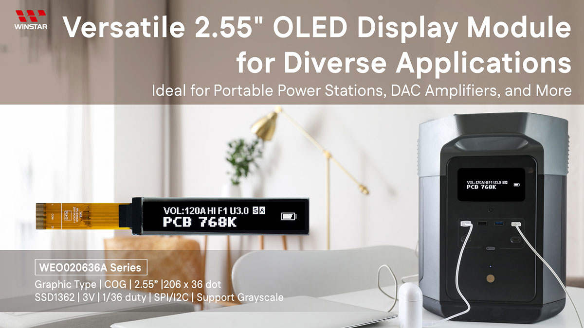
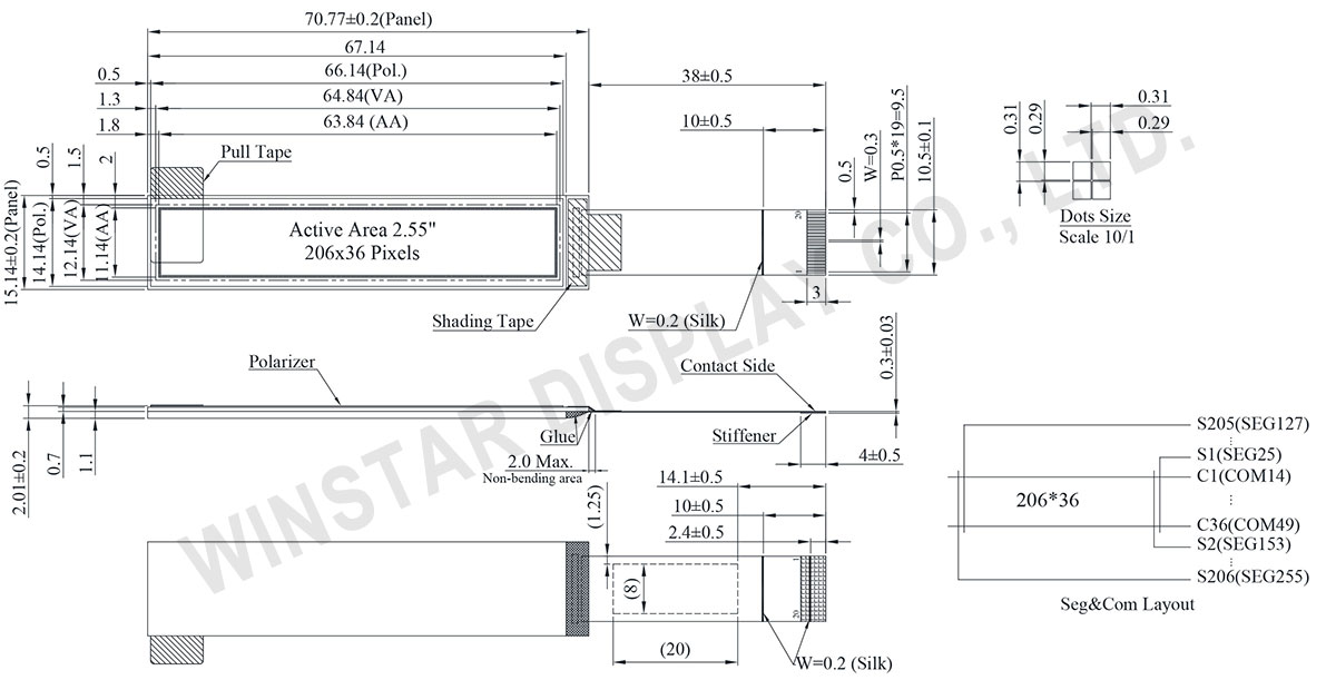
WINSTAR初の2.55インチで解像度206x36ドットであるOLED モジュールWEO020636A シリーズを紹介させて頂きます。このCOG (Chip on Glass) グラフィック OLED ディスプレイは、外形寸法が70.77 x 15.14 mmで、アクティブ領域が63.84 x 11.14 mmです。他の仕様は以下通りとなります。
WEO020636A OLED ディスプレイは、ポータブル DAC (デジタル アナログ コンバータ) ヘッドフォン アンプなどのアプリケーションに最適です。コンパクトなサイズと優れた視覚的鮮明さにより、モバイル デバイス、産業機器、医療機器、民生用電子機器に適しています。
ハンドヘルド デバイスのユーザー インターフェイスを強化する場合でも、産業環境で重要な視覚フィードバックを提供する場合でも、WEO020636A は、幅広い温度範囲にわたって信頼性の高いパフォーマンスと耐久性を保証します。
| 項目 | 標準値 | 単位 |
|---|---|---|
| ドットマトリックス(解像度) | 206 x 36 Dots | - |
| モジュールサイズ | 70.77 x 15.14 x 2.01 | mm |
| 有効エリア | 63.84 x 11.14 | mm |
| ドットサイズ | 0.29 x 0.29 | mm |
| ドットピッチ | 0.31 x 0.31 | mm |
| 表示モード | パッシブマトリクス | |
| 発光色 | モノクロ | |
| 駆動方法 | 1/36 Duty | |
| グレースケール | 4 Bits | |
| IC | SSD1362 | |
| インターフェース | 3-Wire SPI、4-Wire SPI、I2C | |
| 表示サイズ(対角線) | 2.55 インチ | |
| パラメーター | 記号 | 最小値 | 最大値 | 単位 |
|---|---|---|---|---|
| 電源電圧 | VDD | -0.5 | 2.75 | V |
| 電源電圧 | VCI | -0.3 | 5.5 | V |
| 電源電圧 | VDDIO | -0.5 | 5.5 | V |
| 電源電圧 | VCC | 7 | 21 | V |
| 操作温度 | TOP | -40 | +80 | °C |
| 保存温度 | TSTG | -40 | +85 | °C |
| 項目 | 記号 | 条件 | 最小値 | 典型値 | 最大値 | 単位 |
|---|---|---|---|---|---|---|
| 表示用電源電圧 | VCC | - | 10.0 | 12.0 | 12.5 | V |
| 低電圧電源 | VCI | - | 1.65 | - | 3.5 | V |
| I/Oピン用電源 | VDDIO | - | 1.65 | - | VCI | V |
| ロジック電源電圧 | VDD | - | 1.65 | - | 2.6 | V |
| 高レベル入力電圧 | VIH | - | 0.8×VDDIO | - | - | V |
| 低レベル入力電圧 | VIL | - | - | - | 0.2×VDDIO | V |
| 高レベル出力電圧 | VOH | - | 0.9×VDDIO | - | - | V |
| 低レベル出力電圧 | VOL | - | - | - | 0.1×VDDIO | V |
| Display 50% Pixel on | ICC | VCC =12V | - | 25 | 35 | mA |
| No. | 記号 | 功能 | ||||||||
|---|---|---|---|---|---|---|---|---|---|---|
| 1 | VCC | Power supply for panel driving voltage. This is also the most positive power voltage supply pin. It is supplied by external high voltage source. | ||||||||
| 2 | VCOMH | COM signal deselected voltage level. A capacitor should be connected between this pin and VSS. No external power supply is allowed to connect to this pin. |
||||||||
| 3 | VP | This pin is the segment pre-charge voltage reference pin. A capacitor should be connected between this pin and VSS. No external power supply is allowed to connect to this pin. |
||||||||
| 4 | VSL | This is a reserved pin. It should be connected to VLSS externally. | ||||||||
| 5 | VLSS | Analog system ground pin. It must be connected to external ground. | ||||||||
| 6 | VDD | VDD can be supplied externally (within the range of 1.65V to 2.6V) or regulated internally from VCI when VCI is >2.6V.A capacitor should be connected between VDD and VSS under all circumstances. | ||||||||
| 7 | VCI | Low voltage power supply. VCI must always be equal to or higher than VDD and VDDIO. |
||||||||
| 8 | VDDIO | Power supply for interface logic level. It should match with the MCU interface voltage level and must be connected to external source. | ||||||||
| 9 | CS# | This pin is the chip select input connecting to the MCU. The chip is enabled for MCU communication only when CS# is pulled Low (active Low).In I2C mode, this pin must be connected to VSS. |
||||||||
| 10 | RES# | This pin is reset signal input. When the pin is pulled Low, initialization of the chip is executed. Keep this pin pull HIGH during normal operation. |
||||||||
| 11 | D/C# | This pin is Data/Command control pin connecting to the MCU. When the pin is pulled HIGH, the data will be interpreted as data. When the pin is pulled LOW, the data will be transferred to a command register. In I2C mode, this pin acts as SA0 for slave address selection. When 3-wire serial interface is selected, this pin must be connected to VSS. |
||||||||
| 12 | D0 | These pins are bi-directional data bus connecting to the MCU data bus. Unused pins are recommended to tie Low. When serial interface mode is selected,D0 will be the serial clock input: SCLK;D1 will be the serial data input: SID. When I2C mode is selected, D2, D1 should be tied together and serve as SDAout, SDAin in application and D0 is the serial clock input, SCL. |
||||||||
| 13 | D1 | |||||||||
| 14 | D2 | |||||||||
| 15 | BS0 | MCU bus interface selection pins.
|
||||||||
| 16 | BS1 | |||||||||
17 |
VSS | Ground pin. | ||||||||
| 18 | IREF | When external IREF is used, a resistor should be connected between this pin and VSS to maintain current of around 18.75uA. When internal IREF is used, this pin should be kept NC. |
||||||||
| 19~20 | VCC | Power supply for panel driving voltage. This is also the most positive power voltage supply pin. It is supplied by external high voltage source. |

「すべてのクッキーを許可」をクリックすると、サイトのナビゲーションを向上させ、サイト使用状況を分析し、マーケティングおよびパフォーマンスの取り組みを支援するために、クッキーをデバイスに保存することに同意したことになります。この件に関する詳細情報は、ポリシーをご覧ください。プライバシーポリシー