이 있는 - WF24MTLAJDNT0")

우리는 귀하의 프라이버시를 소중히 여깁니다
"모든 쿠키 허용"을 클릭하면 사이트 탐색을 개선하고, 사이트 사용을 분석하며, 마케팅 및 성능 노력에 도움을 주기 위해 쿠키를 귀하의 장치에 저장하는 데 동의한 것으로 간주됩니다. 이 주제에 대한 추가 정보는 당사의 정책에서 확인할 수 있습니다. 개인정보 보호정책

 - WEO020636A")
 - WEO020636A")
 - WEO020636A")
 - WEO020636A")
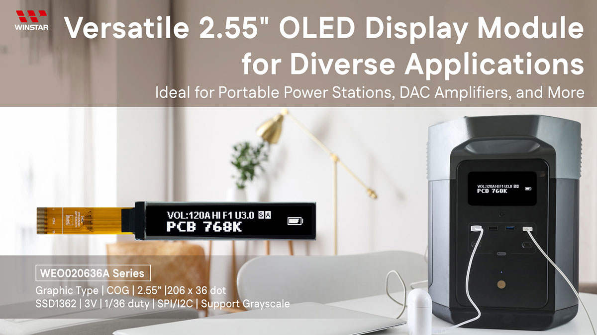
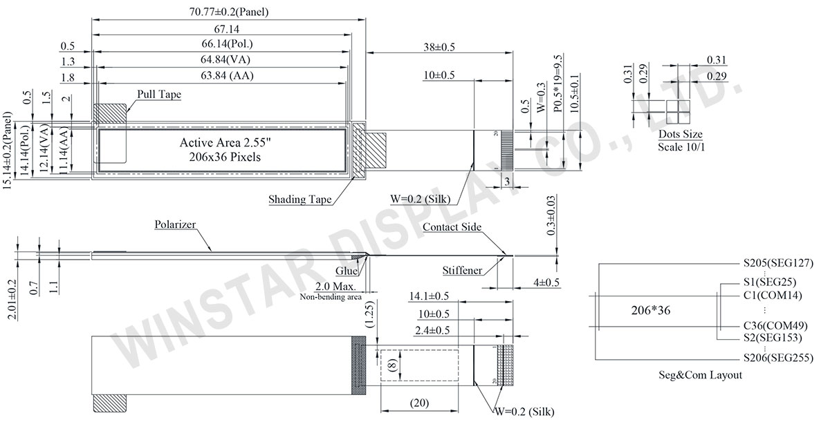
WEO020636A 시리즈는 윈스타의 첫 번째 2.55인치 해상도 206x36 도트의 OLED 모듈입니다. 이 COG (Glass 위 칩) 그래픽 OLED 디스플레이는 70.77 x 15.14 mm의 외형 치수와 63.84 x 11.14 mm의 유효 영역을 가지고 있어 정밀한 시각적 표현을 제공합니다.
WEO020636A OLED 디스플레이는 휴대용 DAC (디지털-아날로그 변환기) 헤드폰 앰프, 휴대용 전원 공급 장치 및 라디오 응용 프로그램을 포함한 다양한 응용 분야에 이상적입니다. 그의 소형 크기와 우수한 시각적 선명도는 모바일 장치, 산업 장비, 의료 장비 및 소비자 전자 제품에 적합합니다. 이 디스플레이의 COG 구조와 SPI 및 I2C 인터페이스와의 호환성은 다양한 디지털 환경에 신속하게 통합되도록 돕습니다.
휴대용 장치에서 사용자 인터페이스를 개선하거나 산업 환경에서 중요한 시각적 피드백을 제공할 때, WEO020636A는 넓은 온도 범위에서 신뢰성 있는 성능과 내구성을 보장합니다.
| 항목 | 치수 | 단위 |
|---|---|---|
| 표시 형식 | 206 x 36 Dots | - |
| 모듈 치수 | 70.77 x 15.14 x 2.01 | mm |
| 활성 영역 | 63.84 x 11.14 | mm |
| 도트 크기 | 0.29 x 0.29 | mm |
| 도트 피치 | 0.31 x 0.31 | mm |
| 디스플레이 모드 | 패시브 매트릭스 | |
| 디스플레이 색상 | Monochrome | |
| 듀티 | 1/36 Duty | |
| 그레이스케일 | 4 Bits | |
| IC | SSD1362 | |
| 인터페이스 | 3-Wire SPI、4-Wire SPI、I2C | |
| 크기 (대각선) | 2.55 인치 | |
| 항목 | 기호 | 최소값 | 최대값 | 단위 |
|---|---|---|---|---|
| Supply Voltage | VDD | -0.5 | 2.75 | V |
| Supply Voltage | VCI | -0.3 | 5.5 | V |
| Supply Voltage | VDDIO | -0.5 | 5.5 | V |
| Supply Voltage | VCC | 7 | 21 | V |
| 작동 온도 | TOP | -40 | +80 | °C |
| 보관 온도 | TSTG | -40 | +85 | °C |
| 항목 | 기호 | 조건 | 최소값 | 대표값 | 최대값 | 단위 |
|---|---|---|---|---|---|---|
| Supply Voltage for Display | VCC | - | 10.0 | 12.0 | 12.5 | V |
| Low voltage power supply | VCI | - | 1.65 | - | 3.5 | V |
| Power supply for I/O pins | VDDIO | - | 1.65 | - | VCI | V |
| Logic Supply Voltage | VDD | - | 1.65 | - | 2.6 | V |
| High Level Input | VIH | - | 0.8×VDDIO | - | - | V |
| Low Level Input | VIL | - | - | - | 0.2×VDDIO | V |
| High Level Output | VOH | - | 0.9×VDDIO | - | - | V |
| Low Level Output | VOL | - | - | - | 0.1×VDDIO | V |
| Display 50% Pixel on | ICC | VCC =12V | - | 25 | 35 | mA |
| No. | 기호 | 기능 | ||||||||
|---|---|---|---|---|---|---|---|---|---|---|
| 1 | VCC | Power supply for panel driving voltage. This is also the most positive power voltage supply pin. It is supplied by external high voltage source. | ||||||||
| 2 | VCOMH | COM signal deselected voltage level. A capacitor should be connected between this pin and VSS. No external power supply is allowed to connect to this pin. |
||||||||
| 3 | VP | This pin is the segment pre-charge voltage reference pin. A capacitor should be connected between this pin and VSS. No external power supply is allowed to connect to this pin. |
||||||||
| 4 | VSL | This is a reserved pin. It should be connected to VLSS externally. | ||||||||
| 5 | VLSS | Analog system ground pin. It must be connected to external ground. | ||||||||
| 6 | VDD | VDD can be supplied externally (within the range of 1.65V to 2.6V) or regulated internally from VCI when VCI is >2.6V.A capacitor should be connected between VDD and VSS under all circumstances. | ||||||||
| 7 | VCI | Low voltage power supply. VCI must always be equal to or higher than VDD and VDDIO. |
||||||||
| 8 | VDDIO | Power supply for interface logic level. It should match with the MCU interface voltage level and must be connected to external source. | ||||||||
| 9 | CS# | This pin is the chip select input connecting to the MCU. The chip is enabled for MCU communication only when CS# is pulled Low (active Low).In I2C mode, this pin must be connected to VSS. |
||||||||
| 10 | RES# | This pin is reset signal input. When the pin is pulled Low, initialization of the chip is executed. Keep this pin pull HIGH during normal operation. |
||||||||
| 11 | D/C# | This pin is Data/Command control pin connecting to the MCU. When the pin is pulled HIGH, the data will be interpreted as data. When the pin is pulled LOW, the data will be transferred to a command register. In I2C mode, this pin acts as SA0 for slave address selection. When 3-wire serial interface is selected, this pin must be connected to VSS. |
||||||||
| 12 | D0 | These pins are bi-directional data bus connecting to the MCU data bus. Unused pins are recommended to tie Low. When serial interface mode is selected,D0 will be the serial clock input: SCLK;D1 will be the serial data input: SID. When I2C mode is selected, D2, D1 should be tied together and serve as SDAout, SDAin in application and D0 is the serial clock input, SCL. |
||||||||
| 13 | D1 | |||||||||
| 14 | D2 | |||||||||
| 15 | BS0 | MCU bus interface selection pins.
|
||||||||
| 16 | BS1 | |||||||||
17 |
VSS | Ground pin. | ||||||||
| 18 | IREF | When external IREF is used, a resistor should be connected between this pin and VSS to maintain current of around 18.75uA. When internal IREF is used, this pin should be kept NC. |
||||||||
| 19~20 | VCC | Power supply for panel driving voltage. This is also the most positive power voltage supply pin. It is supplied by external high voltage source. |

"모든 쿠키 허용"을 클릭하면 사이트 탐색을 개선하고, 사이트 사용을 분석하며, 마케팅 및 성능 노력에 도움을 주기 위해 쿠키를 귀하의 장치에 저장하는 데 동의한 것으로 간주됩니다. 이 주제에 대한 추가 정보는 당사의 정책에서 확인할 수 있습니다. 개인정보 보호정책