我们重视您的隐私
通过点击「允许所有 Cookie」,代表您同意在您的设备上存储 Cookie 以增强网站浏览体验、分析网站使用情况并协助我们的营销和网站效能优化工作。您可以在我们的隐私权政策中找到有关于此的更多信息。
 - WEO020636A")
 - WEO020636A")
 - WEO020636A")
 - WEO020636A")
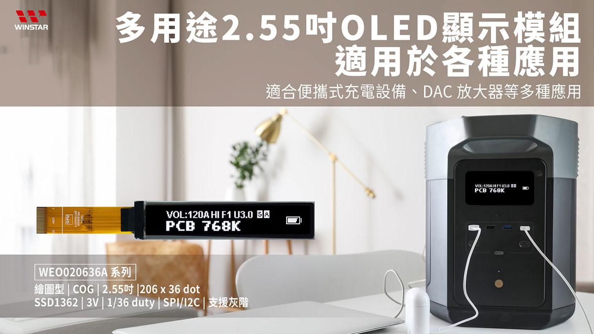
WEO020636A 系列是华凌首次发表的规格 2.55 寸 OLED 显示模块,分辨率为 206x36 dots。这款 COG(Chip on Glass)绘图型 OLED 显示器的外形尺寸为 70.77 x 15.14 mm,有效显示区域为 63.84 x 11.14 mm,提供精确的视觉表现。
WEO020636A OLED 显示器非常适合于多种应用,包括随身型 DAC (Digital-to-Analog Converter) 耳扩、便携式充电设备、小型音响。其纤薄的尺寸和出色的视觉清晰度,使其适用于手持装置、工业设备、医疗设备和消费电子产品。该显示器的 COG 结构及其对 SPI 和 I2C 接口的兼容性,能够无缝整合到各种数字环境中。
增强视觉表现:无论是在手持装置中增强用户接口,还是在工业设置中提供重要的视觉反馈,WEO020636A 都能在广泛的温度范围内保证可靠的性能和耐用性。
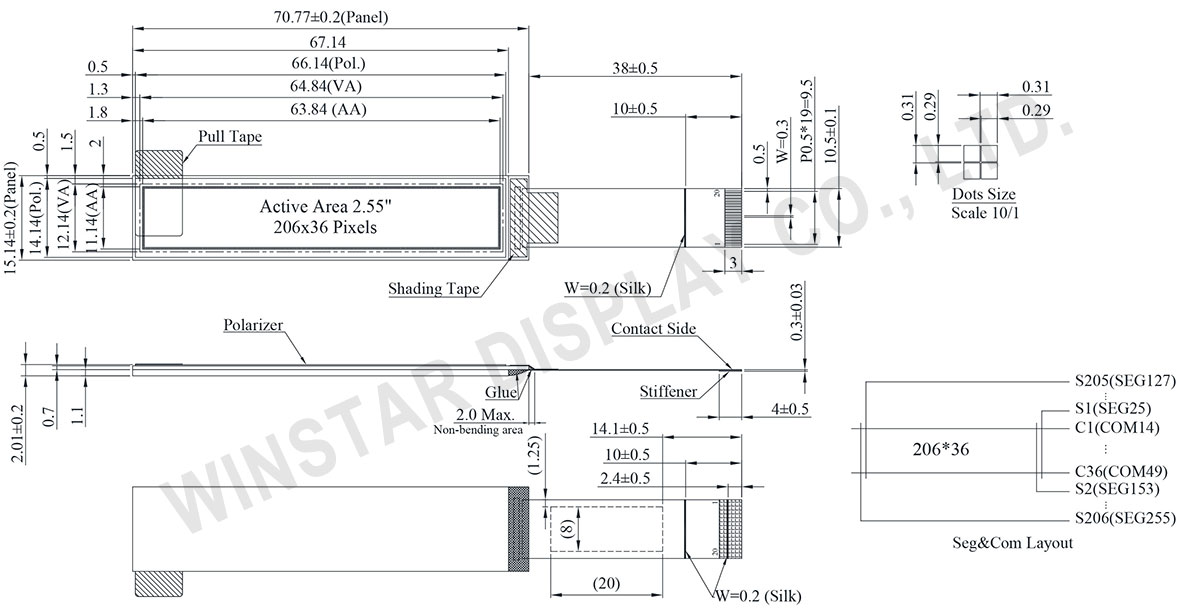
| 项目 | 标准尺寸 | 单位 |
|---|---|---|
| 点阵(分辨率) | 206 x 36 Dots | - |
| 模块尺寸 | 70.77 x 15.14 x 2.01 | mm |
| 有效区域 | 63.84 x 11.14 | mm |
| 点大小 | 0.29 x 0.29 | mm |
| 点间距 | 0.31 x 0.31 | mm |
| 显示模式 | 被动矩阵 | |
| 发光颜色 | 单色 | |
| 驱动方式 | 1/36 Duty | |
| 灰阶 | 4 Bits | |
| IC | SSD1362 | |
| 接口 | 3-Wire SPI、4-Wire SPI、I2C | |
| 显示尺寸(对角线) | 2.55 inch | |
| 参数 | 符号 | 最小值 | 最大值 | 单位 |
|---|---|---|---|---|
| 供电电压 | VDD | -0.5 | 2.75 | V |
| 供电电压 | VCI | -0.3 | 5.5 | V |
| 供电电压 | VDDIO | -0.5 | 5.5 | V |
| 供电电压 | VCC | 7 | 21 | V |
| 工作温度 | TOP | -40 | +80 | °C |
| 储存温度 | TSTG | -40 | +85 | °C |
| 项目 | 符号 | 条件 | 最小值 | 典型值 | 最大值 | 单位 |
|---|---|---|---|---|---|---|
| 显示电压 | VCC | - | 10.0 | 12.0 | 12.5 | V |
| 低电压电源 | VCI | - | 1.65 | - | 3.5 | V |
| I/O pins 电源 | VDDIO | - | 1.65 | - | VCI | V |
| 逻辑电源电压 | VDD | - | 1.65 | - | 2.6 | V |
| 输入高电压 | VIH | - | 0.8×VDDIO | - | - | V |
| 输入低电压 | VIL | - | - | - | 0.2×VDDIO | V |
| 输出高电压 | VOH | - | 0.9×VDDIO | - | - | V |
| 输出低电压 | VOL | - | - | - | 0.1×VDDIO | V |
| Display 50% Pixel on | ICC | VCC =12V | - | 25 | 35 | mA |
| No. | 符号 | 功能 | ||||||||
|---|---|---|---|---|---|---|---|---|---|---|
| 1 | VCC | Power supply for panel driving voltage. This is also the most positive power voltage supply pin. It is supplied by external high voltage source. | ||||||||
| 2 | VCOMH | COM signal deselected voltage level. A capacitor should be connected between this pin and VSS. No external power supply is allowed to connect to this pin. |
||||||||
| 3 | VP | This pin is the segment pre-charge voltage reference pin. A capacitor should be connected between this pin and VSS. No external power supply is allowed to connect to this pin. |
||||||||
| 4 | VSL | This is a reserved pin. It should be connected to VLSS externally. | ||||||||
| 5 | VLSS | Analog system ground pin. It must be connected to external ground. | ||||||||
| 6 | VDD | VDD can be supplied externally (within the range of 1.65V to 2.6V) or regulated internally from VCI when VCI is >2.6V.A capacitor should be connected between VDD and VSS under all circumstances. | ||||||||
| 7 | VCI | Low voltage power supply. VCI must always be equal to or higher than VDD and VDDIO. |
||||||||
| 8 | VDDIO | Power supply for interface logic level. It should match with the MCU interface voltage level and must be connected to external source. | ||||||||
| 9 | CS# | This pin is the chip select input connecting to the MCU. The chip is enabled for MCU communication only when CS# is pulled Low (active Low).In I2C mode, this pin must be connected to VSS. |
||||||||
| 10 | RES# | This pin is reset signal input. When the pin is pulled Low, initialization of the chip is executed. Keep this pin pull HIGH during normal operation. |
||||||||
| 11 | D/C# | This pin is Data/Command control pin connecting to the MCU. When the pin is pulled HIGH, the data will be interpreted as data. When the pin is pulled LOW, the data will be transferred to a command register. In I2C mode, this pin acts as SA0 for slave address selection. When 3-wire serial interface is selected, this pin must be connected to VSS. |
||||||||
| 12 | D0 | These pins are bi-directional data bus connecting to the MCU data bus. Unused pins are recommended to tie Low. When serial interface mode is selected,D0 will be the serial clock input: SCLK;D1 will be the serial data input: SID. When I2C mode is selected, D2, D1 should be tied together and serve as SDAout, SDAin in application and D0 is the serial clock input, SCL. |
||||||||
| 13 | D1 | |||||||||
| 14 | D2 | |||||||||
| 15 | BS0 | MCU bus interface selection pins.
|
||||||||
| 16 | BS1 | |||||||||
17 |
VSS | Ground pin. | ||||||||
| 18 | IREF | When external IREF is used, a resistor should be connected between this pin and VSS to maintain current of around 18.75uA. When internal IREF is used, this pin should be kept NC. |
||||||||
| 19~20 | VCC | Power supply for panel driving voltage. This is also the most positive power voltage supply pin. It is supplied by external high voltage source. |

通过点击「允许所有 Cookie」,代表您同意在您的设备上存储 Cookie 以增强网站浏览体验、分析网站使用情况并协助我们的营销和网站效能优化工作。您可以在我们的隐私权政策中找到有关于此的更多信息。