 - WEX025664B-CTP")

 - WEN025664B")
우리는 귀하의 프라이버시를 소중히 여깁니다
"모든 쿠키 허용"을 클릭하면 사이트 탐색을 개선하고, 사이트 사용을 분석하며, 마케팅 및 성능 노력에 도움을 주기 위해 쿠키를 귀하의 장치에 저장하는 데 동의한 것으로 간주됩니다. 이 주제에 대한 추가 정보는 당사의 정책에서 확인할 수 있습니다. 개인정보 보호정책

 - WEN025664B-CTP")
 - WEN025664B-CTP")
 - WEN025664B-CTP")
 - WEN025664B-CTP")
 - WEN025664B-CTP")
 - WEN025664B-CTP")
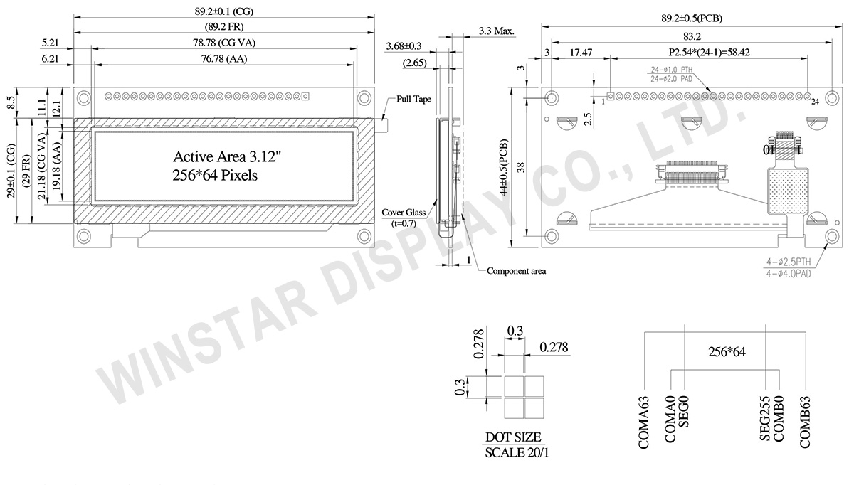
WEN025664B-CTP는 3.12인치 COF 구조의 그래픽 OLED 디스플레이 모듈로, 정전식 터치 패널(CTP)이 통합되어 있으며 해상도는 256×64입니다. SSD1322 드라이버 IC를 탑재하고, 6800/8080 8비트 병렬 및 3/4선 SPI 인터페이스를 지원합니다.
본 모듈은 4비트 그레이스케일을 지원하며, 3V 로직 전원과 1/64 듀티 방식으로 동작합니다. 터치 패널은 FT6336U를 사용하며, I2C 인터페이스와 1포인트 터치를 지원합니다. 패널 표면은 노멀 글레어 타입입니다.
본 제품은 PCB가 통합된 구조로 추가적인 PCB 설계 없이 와이어 연결로 바로 적용할 수 있습니다. 전원 회로와 장착 홀 설계를 통해 시스템 통합 및 기구 설계를 간소화할 수 있습니다.
동작 온도 범위는 -20℃ ~ +70℃, 보관 온도 범위는 -30℃ ~ +80℃입니다. 스마트 홈, 산업 제어, 의료 기기 등 다양한 응용에 적합합니다.
동일 OLED 패널 기반의 다양한 옵션도 제공됩니다:
Data source ref: WEN025664BWPP3D00000
| 항목 | 치수 | 단위 |
|---|---|---|
| 도트 매트릭스 | 256 x 64 Dots | - |
| 모듈 치수 | 89.2 × 44.0 × 7.98 | mm |
| 활성 영역 | 76.78 × 19.18 | mm |
| 픽셀 크기 | 0.278 × 0.278 | mm |
| 픽셀 피치 | 0.3 × 0.3 | mm |
| 디스플레이 모드 | 패시브 매트릭스 | |
| 디스플레이 색상 | 단색 | |
| 구동 듀티 | 1/64 Duty | |
| 그레이스케일 | 4 bits | |
| OLED IC | SSD1322 (COF) | |
| OLED 인터페이스 | 6800, 8080, SPI | |
| 크기 | 3.12 inch | |
| CTP IC | FT6336U | |
| 감지 포인트 | 1 | |
| CTP 인터페이스 | I2C | |
| 표면 | 일반 글레어 | |
| 매개변수 | 기호 | 최소값 | 최대값 | 단위 |
|---|---|---|---|---|
| 디스플레이 전원 전압 | VDD | -0.3 | 4 | V |
| 동작 온도 | TOP | -20 | +70 | °C |
| 보관 온도 | TSTG | -30 | +80 | °C |
| 항목 | 기호 | 조건 | 최소값 | 전형값 | 최대값 | 단위 |
|---|---|---|---|---|---|---|
| 로직 전원 전압 | VDD | - | 2.8 | 3.0 | 3.3 | V |
| 입력 High 전압 | VIH | - | 0.8×VDD | - | VDD | V |
| 입력 Low 전압 | VIL | - | 0 | - | 0.2×VDD | V |
| 출력 High 전압 | VOH | - | 0.9×VDD | - | VDD | V |
| 출력 Low 전압 | VOL | - | 0 | - | 0.1×VDD | V |
| 50% Check Board 동작 전류 | IDD | VDD =3V | - | 150 | 300 | mA |
| Pin Number | 기호 | I/O | 기능 | ||||||||||
|---|---|---|---|---|---|---|---|---|---|---|---|---|---|
| 1 | VSS | P | Ground. | ||||||||||
| 2 | VDD | P | Power Supply for Core Logic Circuit Power supply pin for core logic operation. A capacitor is required to connect between this pin and VSS |
||||||||||
| 3 | N.C. | P | Reserved Pin The N.C. pin between function pins are reserved for compatible and flexible design. |
||||||||||
| 4 | D/C# | I | Data/Command Control This pin is Data/Command control pin connecting to the MCU. When the pin is pulled HIGH, the content at D[7:0] will be interpreted as data. When the pin is pulled LOW, the content at D[7:0] will be interpreted as command. |
||||||||||
| 5 | R/W# (WR#) |
I | Read/Write Select or Write This pin is MCU interface input. When interfacing to a 68XX-series microprocessor, this pin will be used as Read/Write (R/W#) selection input. Pull this pin to “High” for read mode and pull it to “Low” for write mode. When 80XX interface mode is selected, this pin will be the Write (WR#) input. Data write operation is initiated when this pin is pulled low and the CS# is pulled low. When serial mode is selected, this pin must be connected to VSS. |
||||||||||
| 6 | E/RD# | I | Read/Write Enable or Read This pin is MCU interface input. When interfacing to a 68XX-series microprocessor, this pin will be used as the Enable (E) signal. Read/write operation is initiated when this pin is pulled high and the CS# is pulled low. When connecting to an 80XX-microprocessor, this pin receives the Read (RD#) signal. Data read operation is initiated when this pin is pulled low and CS# is pulled low. When serial mode is selected, this pin must be connected to VSS. |
||||||||||
| 7~14 | DB0 | I/O | Host Data Input/Output Bus These pins are 8-bit bi-directional data bus to be connected to the microprocessor’s data bus. When serial mode is selected, D1 will be the serial data input SDIN and D0 will be the serial clock input SCLK. |
||||||||||
| DB1 | |||||||||||||
| DB2 | |||||||||||||
| DB3 | |||||||||||||
| DB4 | |||||||||||||
| DB5 | |||||||||||||
| DB6 | |||||||||||||
| DB7 | |||||||||||||
| 15 | NC | P | Reserved Pin The N.C. pin between function pins are reserved for compatible and flexible design. |
||||||||||
| 16 | RES# | I | This pin is reset signal input. When the pin is pulled LOW, initialization of the chip is executed. Keep this pin pull HIGH during normal operation. |
||||||||||
| 17 | CS# | I | Data/Command Control This pin is the chip select input connecting to the MCU. The chip is enabled for MCU communication only when CS# is pulled LOW. |
||||||||||
| 18 | NC | P | Reserved Pin The N.C. pin between function pins are reserved for compatible and flexible design. |
||||||||||
| 19 | BS1 | I | Communicating Protocol Select These pins are MCU interface selection input. See the following table:
(1) 0 is connected to VSS (2) 1 is connected to VDD |
||||||||||
| 20 | BS0 | ||||||||||||
| 21 | TP_SCK | I | I2C clock input | ||||||||||
| 22 | TP_SDA | I | I2C data input and output | ||||||||||
| 23 | TP_INT | I | External interrupt to the host | ||||||||||
| 24 | TP_RST | I | External Reset, Low is active |

"모든 쿠키 허용"을 클릭하면 사이트 탐색을 개선하고, 사이트 사용을 분석하며, 마케팅 및 성능 노력에 도움을 주기 위해 쿠키를 귀하의 장치에 저장하는 데 동의한 것으로 간주됩니다. 이 주제에 대한 추가 정보는 당사의 정책에서 확인할 수 있습니다. 개인정보 보호정책