 - WEX025664B-CTP")
 - WEN025664B-CTP")
 - WEN025664B")
우리는 귀하의 프라이버시를 소중히 여깁니다
"모든 쿠키 허용"을 클릭하면 사이트 탐색을 개선하고, 사이트 사용을 분석하며, 마케팅 및 성능 노력에 도움을 주기 위해 쿠키를 귀하의 장치에 저장하는 데 동의한 것으로 간주됩니다. 이 주제에 대한 추가 정보는 당사의 정책에서 확인할 수 있습니다. 개인정보 보호정책


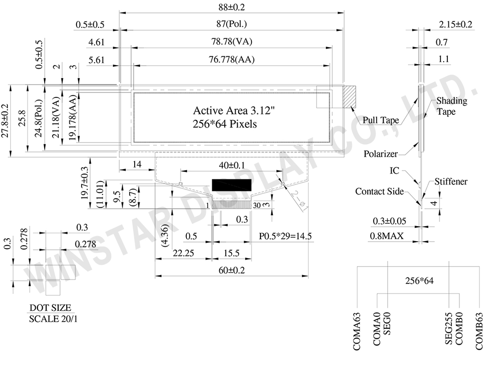
WEX025664B는 해상도 256×64 dots의 3.12인치 COF 구조 그래픽 OLED 디스플레이입니다. SSD1322 드라이버 IC를 탑재하고 있으며, 6800/8080 8-bit 병렬 및 3-/4-wire SPI 인터페이스를 지원합니다. 모듈 외형 크기는 88.0 × 27.8 mm, 표시 영역은 76.778 × 19.178 mm입니다.
본 디스플레이는 4-bit 그레이스케일을 지원하며, 로직 전압은 2.5V (typ.), 1/64 duty 구동 방식을 적용합니다. 10,000:1 명암비를 제공하며, 동작 온도 범위는 -40°C ~ +80°C, 보관 온도 범위는 -40°C ~ +85°C입니다.
WEX025664B 시리즈는 그레이스케일 표현이 가능한 컴팩트 모노크롬 OLED 디스플레이가 필요한 응용에 적합하며, 계측기, 휴대용 장비, POS 시스템, IoT 장치, 통신 장비, 의료 기기 등에 적용할 수 있습니다. 구조 및 터치 옵션에 따라 다음과 같은 관련 모델을 선택할 수 있습니다.
| 항목 | 치수 | 단위 |
|---|---|---|
| 도트 매트릭스 | 256 x 64 Dots | - |
| 모듈 치수 | 88.0 × 27.8 × 2.15 | mm |
| 활성 영역 | 76.778×19.178 | mm |
| 도트 크기 | 0.278×0.278 | mm |
| 도트 피치 | 0.3×0.3 | mm |
| 디스플레이 모드 | 패시브 매트릭스 | |
| 디스플레이 색상 | 단색 | |
| 구동 듀티비 | 1/64 Duty | |
| 그레이스케일 | 4 bits | |
| IC | SSD1322 (COF) | |
| 인터페이스 | 6800, 8080, SPI | |
| 크기 | 3.12 inch | |
| 항목 | 기호 | 최소값 | 최대값 | 단위 |
|---|---|---|---|---|
| 동작 전압 | VCI | -0.3 | 4 | V |
| 논리용 전원 공급 전압 | VDD | -0.5 | 2.75 | V |
| I/O 핀 전원 전압 | VDDIO | -0.5 | VCI | V |
| 디스플레이 전원 공급 전압 | VCC | -0.5 | 20 | V |
| 작동 온도 | TOP | -40 | 80 | °C |
| 보관 온도 | TSTG | -40 | 85 | °C |
| 항목 | 기호 | 조건 | 최소값 | 대표값 | 최대값 | 단위 |
|---|---|---|---|---|---|---|
| 논리용 전원 공급 전압 | VDD | - | 2.4 | 2.5 | 2.6 | V |
| I/O 핀 전원 전압 | VDDIO | - | 1.65 | 3.0 | VCI | V |
| 저전압 전원 공급 | VCI | - | 2.4 | 3.0 | 3.5 | V |
| 디스플레이 전원 공급 전압 | VCC | - | 11.5 | 14.5 | 15 | V |
| 입력 High 전압 | VIH | - | 0.8×VDDIO | - | VDDIO | V |
| 입력 Low 전압 | VIL | - | 0 | - | 0.2×VDDIO | V |
| 출력 High 전압 | VOH | - | 0.9×VDDIO | - | VDDIO | V |
| 출력 Low 전압 | VOL | - | 0 | - | 0.1×VDDIO | V |
| 50% 보드 동작 전류 | ICC | VCC =12V | - | 24 | 32 | mA |
| VCC =14.5V | - | 32 | 42.5 | mA |
| Pin Number | 기호 | I/O | 기능 | ||||||||||
|---|---|---|---|---|---|---|---|---|---|---|---|---|---|
| 1 | N.C. (GND) | P | Ground | ||||||||||
| 2 | VSS | P | Ground. | ||||||||||
| 3 | VCC | P | Power supply for panel driving voltage. This is also the most positive power voltage supply pin. |
||||||||||
| 4 | VCOMH | P | COM signal deselected voltage level. A capacitor should be connected between this pin and VSS. |
||||||||||
| 5 | VLSS | P | Analog system ground pin. | ||||||||||
| 6~13 | D7~D0 | I/O | Host Data Input/Output Bus These pins are 8-bit bi-directional data bus to be connected to the microprocessor’s data bus. When serial mode is selected, D1 will be the serial data input SDIN and D0 will be the serial clock input SCLK. |
||||||||||
| 14 | E/RD# | I | Read/Write Enable or Read This pin is MCU interface input. When interfacing to a 68XX-series microprocessor, this pin will be used as the Enable (E) signal. Read/write operation is initiated when this pin is pulled high and the CS# is pulled low. When connecting to an 80XX-microprocessor, this pin receives the Read (RD#) signal. Data read operation is initiated when this pin is pulled low and CS# is pulled low. When serial mode is selected, this pin must be connected to VSS. |
||||||||||
| 15 | R/W# | I | Read/Write Select or Write This pin is MCU interface input. When interfacing to a 68XX-series microprocessor, this pin will be used as Read/Write (R/W#) selection input. Pull this pin to “High” for read mode and pull it to “Low” for write mode. When 80XX interface mode is selected, this pin will be the Write (WR#) input. Data write operation is initiated when this pin is pulled low and the CS# is pulled low. When serial mode is selected, this pin must be connected to VSS. |
||||||||||
| 16 | BS0 | I | Communicating Protocol Select These pins are MCU interface selection input. See the following table:
(1) 0 is connected to VSS (2) 1 is connected to VDDIO |
||||||||||
| 17 | BS1 | ||||||||||||
| 18 | D/C# | I | Data/Command Control This pin is Data/Command control pin connecting to the MCU. When the pin is pulled HIGH, the content at D[7:0] will be interpreted as data. When the pin is pulled LOW, the content at D[7:0] will be interpreted as command. |
||||||||||
| 19 | CS# | I | Data/Command Control This pin is the chip select input connecting to the MCU. The chip is enabled for MCU communication only when CS# is pulled LOW. |
||||||||||
| 20 | RES# | I | This pin is reset signal input. When the pin is pulled LOW, initialization of the chip is executed. Keep this pin pull HIGH during normal operation. |
||||||||||
| 21 | FR | O | This pin is No Connection pins. Nothing should be connected to this pin. This pin should be left open individually. | ||||||||||
| 22 | IREF | I | Current Reference for Brightness Adjustment This pin is segment current reference pin. A resistor should be connected between this pin and VSS. Set the current lower than 10uA. |
||||||||||
| 23 | N.C. | - | Reserved Pin The N.C. pin between function pins are reserved for compatible and flexible design. |
||||||||||
| 24 | VDDIO | P | Power Supply for I/O Pin It should be matched with the MCU interface voltage level. |
||||||||||
| 25 | VDD | P | Power Supply for Core Logic Circuit Power supply pin for core logic operation. A capacitor is required to connect between this pin and VSS |
||||||||||
| 26 | VCI | P | Power Supply for Operation VCI must always be equal to or higher than VDD and VDDIO. |
||||||||||
| 27 | VSL | P | Voltage Output Low Level for SEG Signal This is segment voltage reference pin. When external VSL is not used, this pin should be left open. When external VSL is used, this pin should connect with resistor and diode to ground. |
||||||||||
| 28 | VLSS | P | Ground of Analog Circuit These are the analog ground pins. They should be connected to VSS externally. |
||||||||||
| 29 | VCC | P | Power Supply for OLED Panel These are the most positive voltage supply pin of the chip. They must be connected to external source. |
||||||||||
| 30 | N.C. (GND) | P | Ground |

"모든 쿠키 허용"을 클릭하면 사이트 탐색을 개선하고, 사이트 사용을 분석하며, 마케팅 및 성능 노력에 도움을 주기 위해 쿠키를 귀하의 장치에 저장하는 데 동의한 것으로 간주됩니다. 이 주제에 대한 추가 정보는 당사의 정책에서 확인할 수 있습니다. 개인정보 보호정책