 - WEA025664A")

私たちはあなたのプライバシーを大切にします
「すべてのクッキーを許可」をクリックすると、サイトのナビゲーションを向上させ、サイト使用状況を分析し、マーケティングおよびパフォーマンスの取り組みを支援するために、クッキーをデバイスに保存することに同意したことになります。この件に関する詳細情報は、ポリシーをご覧ください。プライバシーポリシー

 - WEO025664A")
 - WEO025664A")
 - WEO025664A")
 - WEO025664A")
 - WEO025664A")
 - WEO025664A")
型番 WEO025664A
►グラフィック有機ELモジュール
►結構: COG
►サイズ:2.08インチ
►256x64 ドットマトリックス
►IC:SSD1362
►3V電源電圧
►1/64 duty
►インターフェース: 6800, 8080, SPI, I2C
►発光色: 白色 / 黄色
►グレースケール機能をサポートする
►Other FPC options available in below table
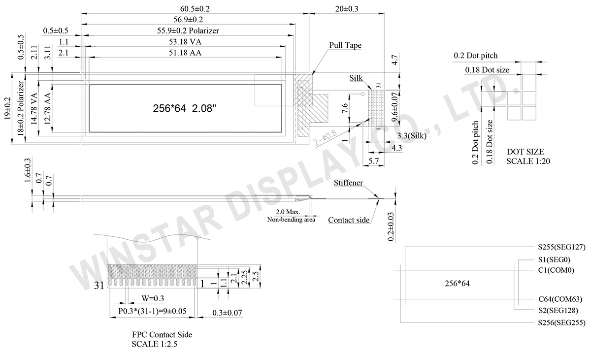
WEO025664Aは、対角2.08インチ、解像度256×64ピクセルのCOG構造グラフィックOLEDディスプレイモジュールです。SSD1362ドライバICを搭載し、6800/8080 8ビットパラレル、I2C、および3線/4線SPIインターフェースに対応しています。また、4ビットグレースケール表示をサポートしています。
本モジュールは3Vロジック電源で動作し、1/64デューティ駆動方式を採用しています。動作温度範囲は-40℃~+80℃、保存温度範囲は-40℃~+85℃です。
WEO025664Aは、厚さわずか1.61mmの薄型COG構造を採用しており、省スペース設計や低消費電力が求められる用途に適しています。スマートホーム機器、計測機器、携帯機器、医療機器などの用途に適しています。
本モデルは、ZIF FPCやHotbarなど複数のFPC/ピンアウト仕様を用意しており、アプリケーション設計に応じた選択が可能です。
 FPC Options
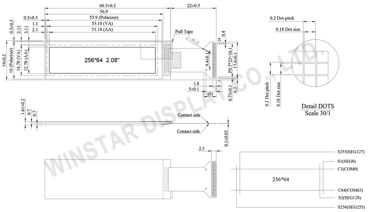
| 項目 | 仕様 | 単位 |
|---|---|---|
| ドットマトリックス(解像度) | 256 x 64 Dots | - |
| 外形寸法 | 60.5 x 19.0 x 1.61 | mm |
| 有効表示エリア | 51.18 x 12.78 | mm |
| ドットサイズ | 0.18 x 0.18 | mm |
| ドットピッチ | 0.2 x 0.2 | mm |
| 表示モード | パッシブマトリクス | |
| 発光色 | モノクロ | |
| 駆動方法 | 1/64 Duty | |
| グレースケール | 4 Bits | |
| IC | SSD1362 | |
| インターフェイス | 3-Wire and 4-Wire SPI, I2C, 6800, 8080 | |
| サイズ | 2.08 インチ | |
| パラメーター | 記号 | 最小値 | 最大値 | 単位 |
|---|---|---|---|---|
| 動作電源電圧 | VCI | -0.5 | 5.5 | V |
| ロジック電源電圧 | VDD | -0.5 | 2.75 | V |
| Display電源電圧 | VCC | -0.5 | 21 | V |
| 操作温度 | TOP | -40 | 80 | °C |
| 保存温度 | TSTG | -40 | 85 | °C |
| 項目 | 記号 | 条件 | 最小値 | 典型値 | 最大値 | 単位 |
|---|---|---|---|---|---|---|
| ロジック電源電圧 | VCI | - | 2.8 | 3.0 | 3.3 | V |
| Display電源電圧 | VCC | - | 11.5 | 12 | 12.5 | V |
| 入力電圧(High) | VIH | - | 0.8×VCI | - | VCI | V |
| 入力電圧(Low) | VIL | - | VSS | - | 0.2×VCI | V |
| 出力電圧(High) | VOH | - | 0.9×VCI | - | VCI | V |
| 出力電圧(Low) | VOL | - | VSS | - | 0.1×VCI | V |
| 50% チェックボード動作電流 | ICC | VCC=12V | - | 15 | 30 | mA |
| No. | 記号 | 説明 | ||||||||||||
|---|---|---|---|---|---|---|---|---|---|---|---|---|---|---|
| 1 | VCC | Power supply for panel driving voltage. This is also the most positive power voltage supply pin. It is supplied by external high voltage source. | ||||||||||||
| 2 | VP | This pin is the segment pre-charge voltage reference pin. A capacitor should be connected between this pin and VSS. No external power supply is allowed to connect to this pin. |
||||||||||||
| 3 | VCOMH | COM signal deselected voltage level. A capacitor should be connected between this pin and VSS. No external power supply is allowed to connect to this pin. |
||||||||||||
| 4 | VDD | Power supply for core logic operation. VDD can be supplied externally (within the range of 1.65V to 2.6V) or regulated internally from VCI when VCI is >2.6V. A capacitor should be connected between VDD and VSS under all circumstances. |
||||||||||||
| 5 | IREF | This pin is the segment output current reference pin. When external IREF is used, a resistor should be connected between this pin and VSS to maintain current of around 18.75uA. When internal IREF is used, this pin should be kept NC. |
||||||||||||
| 6 | VSS | Ground pin. It must be connected to external ground. | ||||||||||||
| 7 | VSS | Ground pin. It must be connected to external ground. | ||||||||||||
| 8 | VCI | Low voltage power supply. VCI must always be equal to or higher than VDD and VDDIO. |
||||||||||||
| 9 | BS0 | MCU bus interface selection pins. Select appropriate logic setting as described in the following table. BS2 and BS1, BS0 are pin select.
|
||||||||||||
| 10 | BS1 | |||||||||||||
| 11 | BS2 | |||||||||||||
| 12 | CS | This pin is the chip select input connecting to the MCU. The chip is enabled for MCU communication only when CS is pulled LOW (active LOW). In I2C mode, this pin must be connected to VSS. |
||||||||||||
| 13 | RES | This pin is reset signal input. When the pin is pulled LOW, initialization of the chip is executed. Keep this pin pull HIGH during normal operation. |
||||||||||||
| 14 | D/C | This pin is Data/Command control pin connecting to the MCU. When the pin is pulled HIGH, the data at D[7:0] will be interpreted as data. When the pin is pulled LOW, the data at D[7:0] will be transferred to a command register. In I2C mode, this pin acts as SA0 for slave address selection. When 3-wire serial interface is selected, this pin must be connected to VSS. |
||||||||||||
| 15 | R/W | This pin is read / write control input pin connecting to the MCU interface. When 6800 interface mode is selected, this pin will be used as Read/Write (R/W) selection input. Read mode will be carried out when this pin is pulled HIGH and write mode when LOW. When 8080 interface mode is selected, this pin will be the Write (WR) input. Data write operation is initiated when this pin is pulled LOW and the chip is selected. When serial or I2C interface is selected, this pin must be connected to VSS. |
||||||||||||
| 16 | RD | This pin is MCU interface input. When 6800 interface mode is selected, this pin will be used as the Enable signal. Read/write operation is initiated when this pin is pulled HIGH and the chip is selected. When 8080 interface mode is selected, this pin receives the Read (RD) signal. Read operation is initiated when this pin is pulled LOW and the chip is selected. When serial or I2C interface is selected, this pin must be connected to VSS. |
||||||||||||
| 17 | D0 | These pins are bi-directional data bus connecting to the MCU data bus. Unused pins are recommended to tie LOW. When serial interface mode is selected, D0 will be the serial clock input: SCLK; D1 will be the serial data input: SID. When I2C mode is selected, D2, D1 should be tied together and serve as SDAout, SDAin in application and D0 is the serial clock input, SCL. |
||||||||||||
| 18 | D1 | |||||||||||||
| 19 | D2 | |||||||||||||
| 20 | D3 | |||||||||||||
| 21 | D4 | |||||||||||||
| 22 | D5 | |||||||||||||
| 23 | D6 | |||||||||||||
| 24 | D7 |
| Drawing | FPC Length | PIN | Pitch | ZIF or HOTBAR FPC | Interface | FPC No. | Create Date |
|---|---|---|---|---|---|---|---|
 |
23 | 24 | 0.7 | HOTBAR | 3-Wire and 4-Wire SPI, I2C, 6800, 8080 | FPC2070002401XXXXX02 | 20180611 |
 |
21 | 31 | 0.3 | ZIF | 3-Wire and 4-Wire SPI, I2C, 6800, 8080 | FPC2030003111XXXXX02 | 20171107 |

「すべてのクッキーを許可」をクリックすると、サイトのナビゲーションを向上させ、サイト使用状況を分析し、マーケティングおよびパフォーマンスの取り組みを支援するために、クッキーをデバイスに保存することに同意したことになります。この件に関する詳細情報は、ポリシーをご覧ください。プライバシーポリシー