 - WEA025664A")
我们重视您的隐私
通过点击「允许所有 Cookie」,代表您同意在您的设备上存储 Cookie 以增强网站浏览体验、分析网站使用情况并协助我们的营销和网站效能优化工作。您可以在我们的隐私权政策中找到有关于此的更多信息。
 - WEO025664A")
 - WEO025664A")
 - WEO025664A")
 - WEO025664A")
 - WEO025664A")
 - WEO025664A")
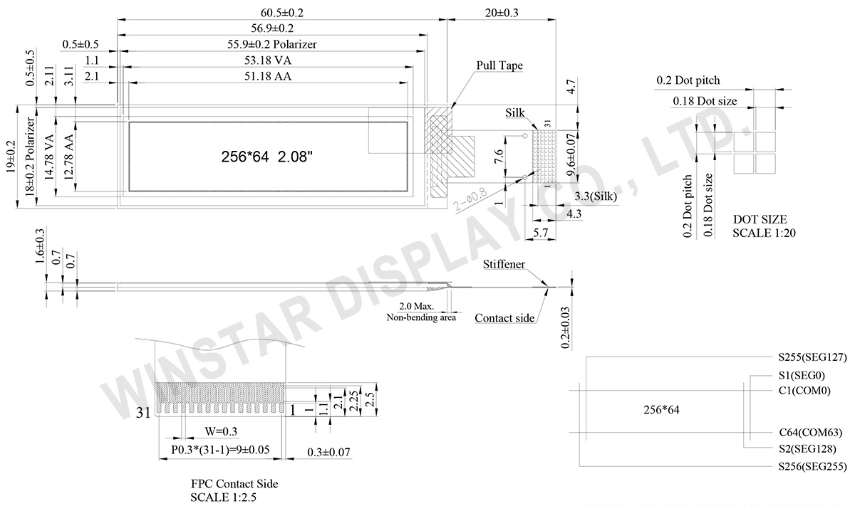
WEO025664A是一款2.08英寸COG结构图形OLED显示模块,分辨率为256×64像素。该模块采用SSD1362驱动IC,支持6800/8080 8位并行接口、I2C以及3线/4线 SPI 串行接口,并支持4位灰阶显示。
该OLED模块采用3V逻辑电压供电,驱动方式为1/64 duty。工作温度范围为-40°C至+80°C,存储温度范围为-40°C至+85°C。
WEO025664A采用紧凑型COG结构,模组厚度仅1.61 mm,适用于空间受限及低功耗应用场景。可广泛应用于智能家居、测量仪器、便携设备以及医疗设备等领域。
该型号提供多种FPC / 引脚方式(pin-out)选项,包括ZIF FPC与Hotbar,可根据不同应用需求选择合适的接口配置。
 FPC Options
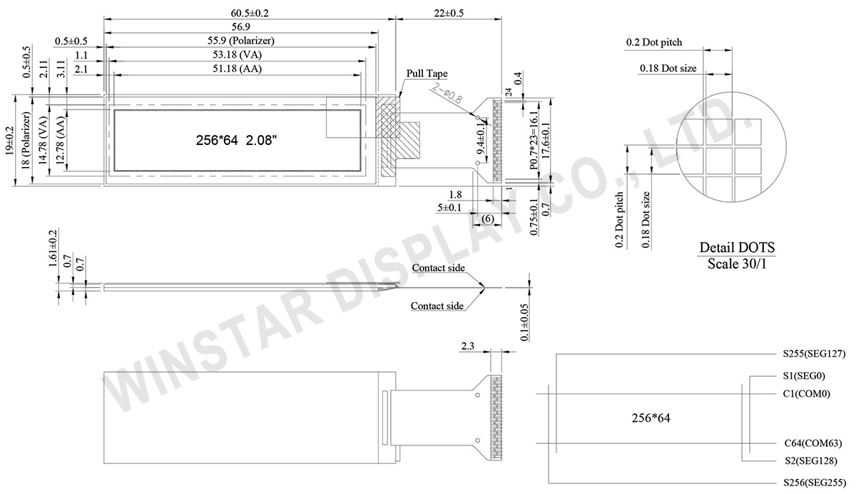
| 项目 | 规格 | 单位 |
|---|---|---|
| 分辨率 | 256 x 64 | Dots |
| 模块尺寸 | 60.5 x 19.0 x 1.61 | mm |
| 有效区域 | 51.18 x 12.78 | mm |
| 像素大小 | 0.18 x 0.18 | mm |
| 像素间距 | 0.2 x 0.2 | mm |
| 显示模式 | 被动矩阵 | |
| 显示颜色 | 单色 | |
| 驱动方式 | 1/64 Duty | |
| 灰阶 | 4 Bits | |
| IC | SSD1362 | |
| 接口 | 3线和4线 SPI, I2C, 6800, 8080 | |
| 尺寸 | 2.08 吋 | |
| 参数 | 符号 | 最小值 | 最大值 | 单位 |
|---|---|---|---|---|
| 工作电源电压 | VCI | -0.5 | 5.5 | V |
| 逻辑电源电压 | VDD | -0.5 | 2.75 | V |
| 显示电源电压 | VCC | -0.5 | 21 | V |
| 工作温度 | TOP | -40 | 80 | °C |
| 储存温度 | TSTG | -40 | 85 | °C |
| 项目 | 符号 | 条件 | 最小值 | 典型值 | 最大值 | 单位 |
|---|---|---|---|---|---|---|
| 逻辑电源电压 | VCI | - | 2.8 | 3.0 | 3.3 | V |
| 逻辑电源电压 | VCC | - | 11.5 | 12 | 12.5 | V |
| 输入高电压 | VIH | - | 0.8×VCI | - | VCI | V |
| 输入高电压 | VIL | - | VSS | - | 0.2×VCI | V |
| 输出高电压 | VOH | - | 0.9×VCI | - | VCI | V |
| 输出低电压 | VOL | - | VSS | - | 0.1×VCI | V |
| 50% 设备运行电流 | ICC | VCC=12V | - | 15 | 30 | mA |
| No. | 符号 | 功能 | ||||||||||||
|---|---|---|---|---|---|---|---|---|---|---|---|---|---|---|
| 1 | VCC | Power supply for panel driving voltage. This is also the most positive power voltage supply pin. It is supplied by external high voltage source. | ||||||||||||
| 2 | VP | This pin is the segment pre-charge voltage reference pin. A capacitor should be connected between this pin and VSS. No external power supply is allowed to connect to this pin. |
||||||||||||
| 3 | VCOMH | COM signal deselected voltage level. A capacitor should be connected between this pin and VSS. No external power supply is allowed to connect to this pin. |
||||||||||||
| 4 | VDD | Power supply for core logic operation. VDD can be supplied externally (within the range of 1.65V to 2.6V) or regulated internally from VCI when VCI is >2.6V. A capacitor should be connected between VDD and VSS under all circumstances. |
||||||||||||
| 5 | IREF | This pin is the segment output current reference pin. When external IREF is used, a resistor should be connected between this pin and VSS to maintain current of around 18.75uA. When internal IREF is used, this pin should be kept NC. |
||||||||||||
| 6 | VSS | Ground pin. It must be connected to external ground. | ||||||||||||
| 7 | VSS | Ground pin. It must be connected to external ground. | ||||||||||||
| 8 | VCI | Low voltage power supply. VCI must always be equal to or higher than VDD and VDDIO. |
||||||||||||
| 9 | BS0 | MCU bus interface selection pins. Select appropriate logic setting as described in the following table. BS2 and BS1, BS0 are pin select.
|
||||||||||||
| 10 | BS1 | |||||||||||||
| 11 | BS2 | |||||||||||||
| 12 | CS | This pin is the chip select input connecting to the MCU. The chip is enabled for MCU communication only when CS is pulled LOW (active LOW). In I2C mode, this pin must be connected to VSS. |
||||||||||||
| 13 | RES | This pin is reset signal input. When the pin is pulled LOW, initialization of the chip is executed. Keep this pin pull HIGH during normal operation. |
||||||||||||
| 14 | D/C | This pin is Data/Command control pin connecting to the MCU. When the pin is pulled HIGH, the data at D[7:0] will be interpreted as data. When the pin is pulled LOW, the data at D[7:0] will be transferred to a command register. In I2C mode, this pin acts as SA0 for slave address selection. When 3-wire serial interface is selected, this pin must be connected to VSS. |
||||||||||||
| 15 | R/W | This pin is read / write control input pin connecting to the MCU interface. When 6800 interface mode is selected, this pin will be used as Read/Write (R/W) selection input. Read mode will be carried out when this pin is pulled HIGH and write mode when LOW. When 8080 interface mode is selected, this pin will be the Write (WR) input. Data write operation is initiated when this pin is pulled LOW and the chip is selected. When serial or I2C interface is selected, this pin must be connected to VSS. |
||||||||||||
| 16 | RD | This pin is MCU interface input. When 6800 interface mode is selected, this pin will be used as the Enable signal. Read/write operation is initiated when this pin is pulled HIGH and the chip is selected. When 8080 interface mode is selected, this pin receives the Read (RD) signal. Read operation is initiated when this pin is pulled LOW and the chip is selected. When serial or I2C interface is selected, this pin must be connected to VSS. |
||||||||||||
| 17 | D0 | These pins are bi-directional data bus connecting to the MCU data bus. Unused pins are recommended to tie LOW. When serial interface mode is selected, D0 will be the serial clock input: SCLK; D1 will be the serial data input: SID. When I2C mode is selected, D2, D1 should be tied together and serve as SDAout, SDAin in application and D0 is the serial clock input, SCL. |
||||||||||||
| 18 | D1 | |||||||||||||
| 19 | D2 | |||||||||||||
| 20 | D3 | |||||||||||||
| 21 | D4 | |||||||||||||
| 22 | D5 | |||||||||||||
| 23 | D6 | |||||||||||||
| 24 | D7 |
| Drawing | FPC Length | PIN | Pitch | ZIF or HOTBAR FPC | Interface | FPC No. | Create Date |
|---|---|---|---|---|---|---|---|
 |
23 | 24 | 0.7 | HOTBAR | 3-Wire and 4-Wire SPI, I2C, 6800, 8080 | FPC2070002401XXXXX02 | 20180611 |
 |
21 | 31 | 0.3 | ZIF | 3-Wire and 4-Wire SPI, I2C, 6800, 8080 | FPC2030003111XXXXX02 | 20171107 |

通过点击「允许所有 Cookie」,代表您同意在您的设备上存储 Cookie 以增强网站浏览体验、分析网站使用情况并协助我们的营销和网站效能优化工作。您可以在我们的隐私权政策中找到有关于此的更多信息。