 - WEA025664A")
 - WEO012864MX")

우리는 귀하의 프라이버시를 소중히 여깁니다
"모든 쿠키 허용"을 클릭하면 사이트 탐색을 개선하고, 사이트 사용을 분석하며, 마케팅 및 성능 노력에 도움을 주기 위해 쿠키를 귀하의 장치에 저장하는 데 동의한 것으로 간주됩니다. 이 주제에 대한 추가 정보는 당사의 정책에서 확인할 수 있습니다. 개인정보 보호정책

 - WEO025664A")
 - WEO025664A")
 - WEO025664A")
 - WEO025664A")
 - WEO025664A")
 - WEO025664A")
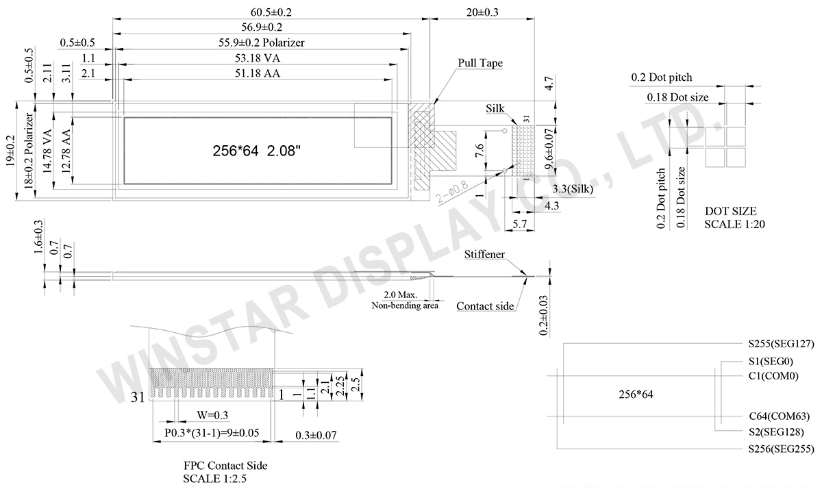
WEO025664A는 대각선 2.08인치, 해상도 256×64의 COG 구조 그래픽 OLED 디스플레이 모듈입니다. SSD1362 드라이버 IC를 기반으로 하며, 6800/8080 8비트 병렬, I2C, 3선/4선 SPI 인터페이스를 지원합니다. 또한 4비트 그레이스케일 표시를 지원합니다.
본 모듈은 3V 로직 전원에서 동작하며 1/64 듀티 구동 방식을 사용합니다. 동작 온도 범위는 -40℃ ~ +80℃, 보관 온도 범위는 -40℃ ~ +85℃입니다.
WEO025664A는 두께 1.61mm의 초슬림 COG 구조로 설계되어 공간 제약이 있는 시스템 및 저전력 애플리케이션에 적합합니다. 스마트 홈 기기, 계측 장비, 휴대용 기기 및 의료 장비 등에 적용할 수 있습니다.
본 모델은 ZIF FPC 및 Hotbar 등 다양한 FPC / 핀 배열 옵션을 제공하여 설계 요구에 맞는 선택이 가능합니다.
 FPC Options
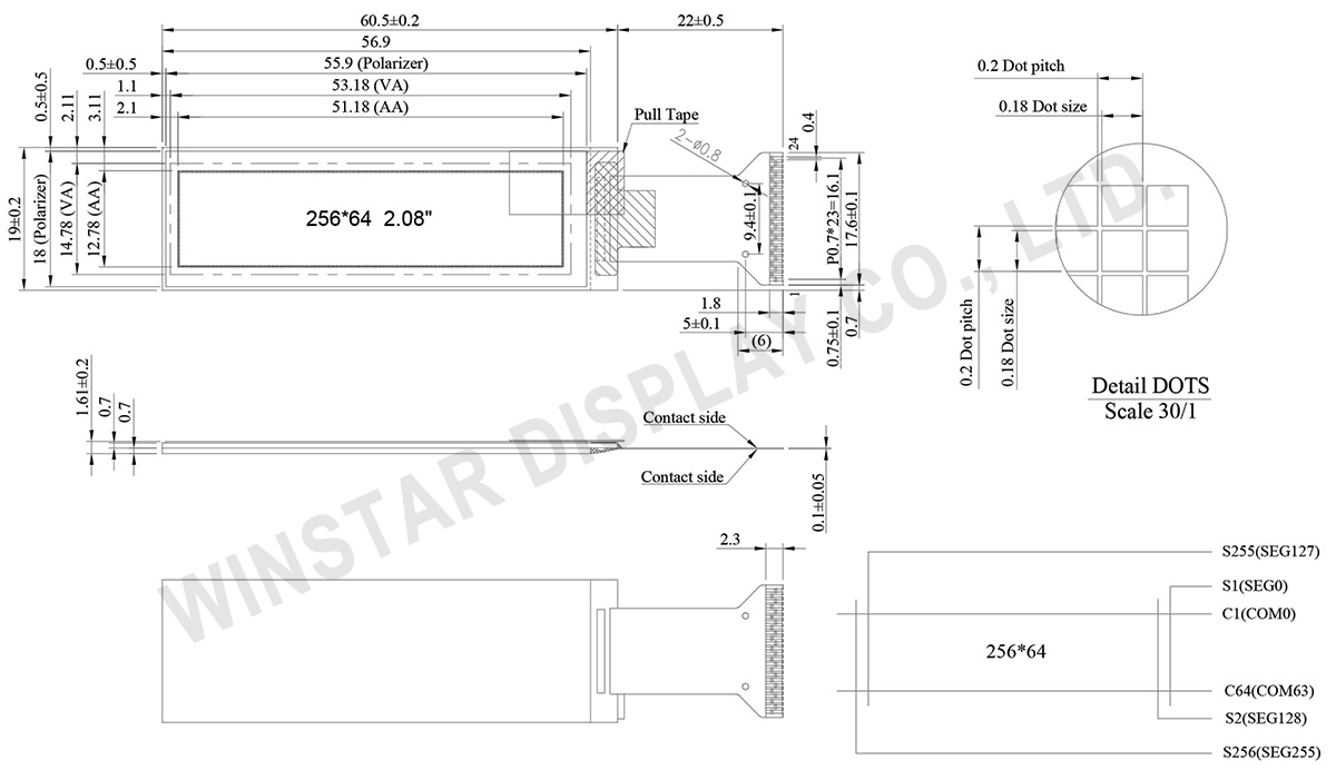
| 항목 | 치수 | 단위 |
|---|---|---|
| 도트 매트릭스 | 256 x 64 Dots | - |
| 모듈 치수 | 60.5 x 19.0 x 1.61 | mm |
| 활성 영역 | 51.18 x 12.78 | mm |
| 도트 크기 | 0.18 x 0.18 | mm |
| 도트 피치 | 0.2 x 0.2 | mm |
| 디스플레이 모드 | 패시브 매트릭스 | |
| 디스플레이 색상 | 단색 | |
| 구동 듀티비 | 1/64 Duty | |
| 그레이스케일 | 4 Bits | |
| IC | SSD1362 | |
| 인터페이스 | 3-Wire and 4-Wire SPI, I2C, 6800, 8080 | |
| 크기 | 2.08 인치 | |
| 항목 | 기호 | 최소값 | 최대값 | 단위 |
|---|---|---|---|---|
| 동작 전압 | VCI | -0.5 | 5.5 | V |
| 로직 전원 전압 | VDD | -0.5 | 2.75 | V |
| 디스플레이 전원 전압 | VCC | -0.5 | 21 | V |
| 동작 온도 | TOP | -40 | 80 | °C |
| 보관 온도 | TSTG | -40 | 85 | °C |
| 항목 | 기호 | 조건 | 최소값 | 대표값 | 최대값 | 단위 |
|---|---|---|---|---|---|---|
| 로직 전원 전압 | VCI | - | 2.8 | 3.0 | 3.3 | V |
| 디스플레이 전원 전압 | VCC | - | 11.5 | 12 | 12.5 | V |
| 입력 High 전압 | VIH | - | 0.8×VCI | - | VCI | V |
| 입력 Low 전압 | VIL | - | VSS | - | 0.2×VCI | V |
| 출력 High 전압 | VOH | - | 0.9×VCI | - | VCI | V |
| 출력 Low 전압 | VOL | - | VSS | - | 0.1×VCI | V |
| 50% 보드 동작 전류 | ICC | VCC=12V | - | 15 | 30 | mA |
| No. | 기호 | 기능 | ||||||||||||
|---|---|---|---|---|---|---|---|---|---|---|---|---|---|---|
| 1 | VCC | Power supply for panel driving voltage. This is also the most positive power voltage supply pin. It is supplied by external high voltage source. | ||||||||||||
| 2 | VP | This pin is the segment pre-charge voltage reference pin. A capacitor should be connected between this pin and VSS. No external power supply is allowed to connect to this pin. |
||||||||||||
| 3 | VCOMH | COM signal deselected voltage level. A capacitor should be connected between this pin and VSS. No external power supply is allowed to connect to this pin. |
||||||||||||
| 4 | VDD | Power supply for core logic operation. VDD can be supplied externally (within the range of 1.65V to 2.6V) or regulated internally from VCI when VCI is >2.6V. A capacitor should be connected between VDD and VSS under all circumstances. |
||||||||||||
| 5 | IREF | This pin is the segment output current reference pin. When external IREF is used, a resistor should be connected between this pin and VSS to maintain current of around 18.75uA. When internal IREF is used, this pin should be kept NC. |
||||||||||||
| 6 | VSS | Ground pin. It must be connected to external ground. | ||||||||||||
| 7 | VSS | Ground pin. It must be connected to external ground. | ||||||||||||
| 8 | VCI | Low voltage power supply. VCI must always be equal to or higher than VDD and VDDIO. |
||||||||||||
| 9 | BS0 | MCU bus interface selection pins. Select appropriate logic setting as described in the following table. BS2 and BS1, BS0 are pin select.
|
||||||||||||
| 10 | BS1 | |||||||||||||
| 11 | BS2 | |||||||||||||
| 12 | CS | This pin is the chip select input connecting to the MCU. The chip is enabled for MCU communication only when CS is pulled LOW (active LOW). In I2C mode, this pin must be connected to VSS. |
||||||||||||
| 13 | RES | This pin is reset signal input. When the pin is pulled LOW, initialization of the chip is executed. Keep this pin pull HIGH during normal operation. |
||||||||||||
| 14 | D/C | This pin is Data/Command control pin connecting to the MCU. When the pin is pulled HIGH, the data at D[7:0] will be interpreted as data. When the pin is pulled LOW, the data at D[7:0] will be transferred to a command register. In I2C mode, this pin acts as SA0 for slave address selection. When 3-wire serial interface is selected, this pin must be connected to VSS. |
||||||||||||
| 15 | R/W | This pin is read / write control input pin connecting to the MCU interface. When 6800 interface mode is selected, this pin will be used as Read/Write (R/W) selection input. Read mode will be carried out when this pin is pulled HIGH and write mode when LOW. When 8080 interface mode is selected, this pin will be the Write (WR) input. Data write operation is initiated when this pin is pulled LOW and the chip is selected. When serial or I2C interface is selected, this pin must be connected to VSS. |
||||||||||||
| 16 | RD | This pin is MCU interface input. When 6800 interface mode is selected, this pin will be used as the Enable signal. Read/write operation is initiated when this pin is pulled HIGH and the chip is selected. When 8080 interface mode is selected, this pin receives the Read (RD) signal. Read operation is initiated when this pin is pulled LOW and the chip is selected. When serial or I2C interface is selected, this pin must be connected to VSS. |
||||||||||||
| 17 | D0 | These pins are bi-directional data bus connecting to the MCU data bus. Unused pins are recommended to tie LOW. When serial interface mode is selected, D0 will be the serial clock input: SCLK; D1 will be the serial data input: SID. When I2C mode is selected, D2, D1 should be tied together and serve as SDAout, SDAin in application and D0 is the serial clock input, SCL. |
||||||||||||
| 18 | D1 | |||||||||||||
| 19 | D2 | |||||||||||||
| 20 | D3 | |||||||||||||
| 21 | D4 | |||||||||||||
| 22 | D5 | |||||||||||||
| 23 | D6 | |||||||||||||
| 24 | D7 |
| 그림 | FPC Length | PIN | Pitch | ZIF or HOTBAR FPC | 인터페이스 | FPC No. | Create Date |
|---|---|---|---|---|---|---|---|
 |
23 | 24 | 0.7 | HOTBAR | 3-Wire and 4-Wire SPI, I2C, 6800, 8080 | FPC2070002401XXXXX02 | 20180611 |
 |
21 | 31 | 0.3 | ZIF | 3-Wire and 4-Wire SPI, I2C, 6800, 8080 | FPC2030003111XXXXX02 | 20171107 |

"모든 쿠키 허용"을 클릭하면 사이트 탐색을 개선하고, 사이트 사용을 분석하며, 마케팅 및 성능 노력에 도움을 주기 위해 쿠키를 귀하의 장치에 저장하는 데 동의한 것으로 간주됩니다. 이 주제에 대한 추가 정보는 당사의 정책에서 확인할 수 있습니다. 개인정보 보호정책