
私たちはあなたのプライバシーを大切にします
「すべてのクッキーを許可」をクリックすると、サイトのナビゲーションを向上させ、サイト使用状況を分析し、マーケティングおよびパフォーマンスの取り組みを支援するために、クッキーをデバイスに保存することに同意したことになります。この件に関する詳細情報は、ポリシーをご覧ください。プライバシーポリシー


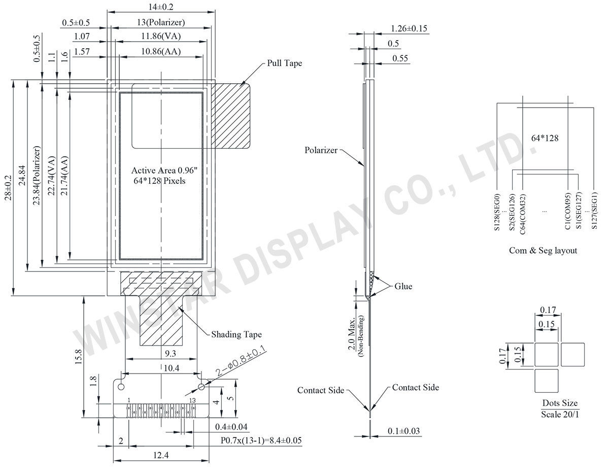
WEO064128A モデルは、消費者向け グラフィック COG OLED ディスプレイで、対角サイズは 0.96 インチ、解像度は 64x128 ピクセル です。この 64x128 OLED ディスプレイ モジュールは、SH1107 IC を内蔵し、4線 SPI および I2C インターフェースに対応しています。ロジック供給電圧は 3V、ディスプレイ供給電圧は 9V です。50% チェックボードパターン時の電流は 8mA @9V VCC(典型値)、駆動率は 1/64 です。
WEO064128A モデルは、SH1107 OLED ディスプレイ と 64x128 の解像度 を搭載しており、ウェアラブルデバイス、携帯機器などのアプリケーションに最適です。動作温度範囲は -30℃ ~ +70℃、保存温度範囲は -30℃ ~ +70℃ で、さまざまな環境条件に適しています。
| 項目 | 仕様 | 単位 |
|---|---|---|
| ドットマトリックス(解像度) | 64 x 128 | Dots |
| 外形寸法 | 14.0 × 28.0 × 1.26 | mm |
| 有効表示エリア | 10.86× 21.74 | mm |
| ピクセルサイズ | 0.15 × 0.15 | mm |
| ピクセルピッチ | 0.17 × 0.17 | mm |
| 表示モード | パッシブマトリクス | |
| 発光色 | モノクロ | |
| 駆動方法 | 1/64 Duty | |
| IC | SH1107 | |
| インターフェイス | 4-wire SPI , I2C | |
| サイズ | 0.96 インチ | |
| パラメーター | 記号 | 最小値 | 最大値 | 単位 |
|---|---|---|---|---|
| ロジック電源電圧 | VDD | -0.3 | 3.6 | V |
| Display電源電圧 | VPP | -0.3 | 17.0 | V |
| 操作温度 | TOP | -30 | +70 | °C |
| 保存温度 | TSTG | -30 | +70 | °C |
| 項目 | 記号 | 条件 | 最小値 | 典型値 | 最大値 | 単位 |
|---|---|---|---|---|---|---|
| ロジック電源電圧 | VDD | - | 1.65 | 3.0 | 3.3 | V |
| Display電源電圧 | VPP | - | 7.0 | 9.0 | 9.5 | V |
| 入力電圧(High) | VIH | - | 0.8×VDD | - | VDD | V |
| 入力電圧(Low) | VIL | - | 0 | - | 0.2×VDD | V |
| 出力電圧(High) | VOH | - | 0.8×VDD | - | VDD | V |
| 出力電圧(Low) | VOL | - | 0 | - | 0.2×VDD | V |
| Operating Current for VCC (50% display ON) | IPP | VPP=9V | - | 8 | 12 | mA |
| No. | 記号 | 説明 |
|---|---|---|
| 1 | NC | Not connected. |
| 2 | VPP | This is the most positive voltage supply pad of the chip. It should be supplied externally. |
| 3 | VCOMH | This is a pad for the voltage output high level for common signals. A capacitor should be connected between this pad and VSS. |
| 4 | VDD | Power supply for logic and input. |
| 5 | IM1 | These are the MPU interface mode select pads. IM1 connect to VDD is I2C interface. IM1 connect to GND is 4-wire SPI interface. |
| 6 | IREF | This is a segment current reference pad. A resistor should be connected between this pad and VSS. Set the current at 15.625uA. |
| 7 | CS | This pad is the chip select input. When CS = “L”, then the chip select becomes active, and data/command I/O is enabled. |
| 8 | RES | This is a reset signal input pad. When RES is set to “L”, the settings are initialized. The reset operation is performed by the RES signal level. |
| 9 | DC | This is the Data/Command control pad that determines whether the data bits are data or a command. DC = “H”: the inputs at D0 to D1 are treated as display data. DC = “L”: the inputs at D0 to D1 are transferred to the command registers. In I2C interface, this pad serves as SA0 to distinguish the different address of OLED driver. |
| 10 | D0 | When the serial interface is selected, then D0 serves as the serial clock input pad (SCL) and D1 serves as the serial data input pad (SI). When the I2C interface is selected, then D0 serves as the serial clock input pad (SCL) and D1 serves as the serial data input pad (SDA). |
| 11 | D1 | |
| 12 | VSS | Ground. |
| 13 | NC | Not connected. |

「すべてのクッキーを許可」をクリックすると、サイトのナビゲーションを向上させ、サイト使用状況を分析し、マーケティングおよびパフォーマンスの取り組みを支援するために、クッキーをデバイスに保存することに同意したことになります。この件に関する詳細情報は、ポリシーをご覧ください。プライバシーポリシー