
우리는 귀하의 프라이버시를 소중히 여깁니다
"모든 쿠키 허용"을 클릭하면 사이트 탐색을 개선하고, 사이트 사용을 분석하며, 마케팅 및 성능 노력에 도움을 주기 위해 쿠키를 귀하의 장치에 저장하는 데 동의한 것으로 간주됩니다. 이 주제에 대한 추가 정보는 당사의 정책에서 확인할 수 있습니다. 개인정보 보호정책


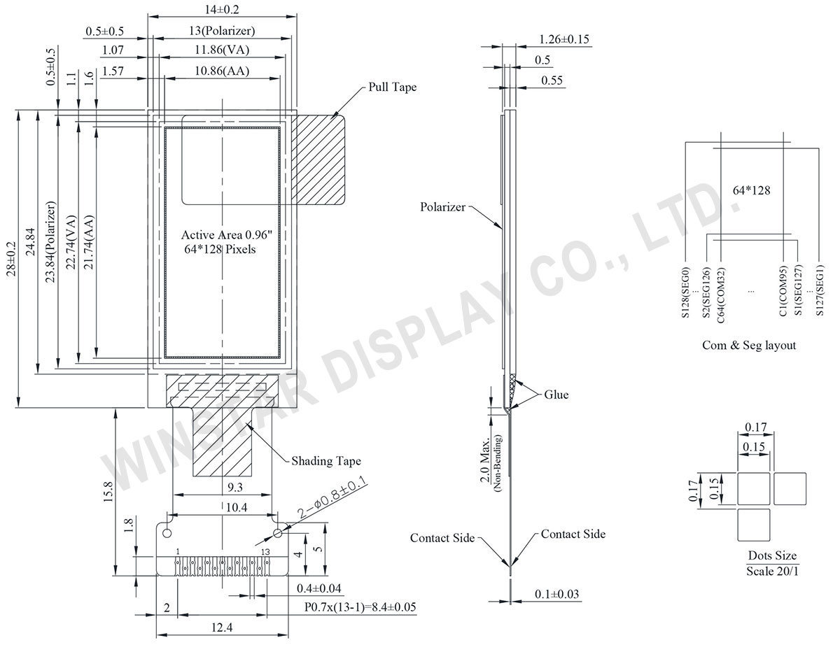
WEO064128A 모델은 소비자용 그래픽 COG OLED 디스플레이로, 대각선 크기는 0.96인치, 해상도는 64x128 픽셀입니다. 이 64x128 OLED 디스플레이 모듈은 SH1107 IC를 내장하고 있으며, 4-wire SPI 및 I2C 인터페이스를 모두 지원합니다. 로직 전압은 3V, 디스플레이 전압은 9V입니다. 50% 체크보드 패턴에서 전류는 8mA @9V VCC (기본 값), 구동 듀티는 1/64입니다.
WEO064128A 모델은 SH1107 OLED 디스플레이와 64x128 해상도를 제공하며, 착용 가능한 장치, 휴대용 장치 등 다양한 애플리케이션에 적합합니다. 이 디스플레이는 –30℃에서 +70℃까지의 온도 범위에서 동작하며, 저장 온도 범위는 –30℃에서 +70℃입니다. 다양한 환경에서 사용할 수 있습니다.
| 항목 | 치수 | 단위 |
|---|---|---|
| 도트 매트릭스 (해상도) | 64 x 128 | Dots |
| 모듈 치수 | 14.0 × 28.0 × 1.26 | mm |
| 활성 영역 | 10.86× 21.74 | mm |
| 도트 크기 | 0.15 × 0.15 | mm |
| 도트 피치 | 0.17 × 0.17 | mm |
| 디스플레이 모드 | 패시브 매트릭스 | |
| 디스플레이 색상 | Monochrome | |
| Drive Duty | 1/64 Duty | |
| IC | SH1107 | |
| 인터페이스 | 4-wire SPI , I2C | |
| 크기 | 0.96 인치 | |
| Parameter | 기호 | 최소값 | 최대값 | 단위 |
|---|---|---|---|---|
| Supply Voltage for Logic | VDD | -0.3 | 3.6 | V |
| Supply Voltage for Display | VPP | -0.3 | 17.0 | V |
| 작동 온도 | TOP | -30 | +70 | °C |
| 보관 온도 | TSTG | -30 | +70 | °C |
| 항목 | 기호 | 조건 | 최소값 | 대표값 | 최대값 | 단위 |
|---|---|---|---|---|---|---|
| Supply Voltage for Logic | VDD | - | 1.65 | 3.0 | 3.3 | V |
| Supply Voltage for Display | VPP | - | 7.0 | 9.0 | 9.5 | V |
| Input High Volt. | VIH | - | 0.8×VDD | - | VDD | V |
| Input Low Volt. | VIL | - | 0 | - | 0.2×VDD | V |
| Output High Volt. | VOH | - | 0.8×VDD | - | VDD | V |
| Output Low Volt. | VOL | - | 0 | - | 0.2×VDD | V |
| Operating Current for VCC (50% display ON) | IPP | VPP=9V | - | 8 | 12 | mA |
| No. | 기호 | 기능 |
|---|---|---|
| 1 | NC | Not connected. |
| 2 | VPP | This is the most positive voltage supply pad of the chip. It should be supplied externally. |
| 3 | VCOMH | This is a pad for the voltage output high level for common signals. A capacitor should be connected between this pad and VSS. |
| 4 | VDD | Power supply for logic and input. |
| 5 | IM1 | These are the MPU interface mode select pads. IM1 connect to VDD is I2C interface. IM1 connect to GND is 4-wire SPI interface. |
| 6 | IREF | This is a segment current reference pad. A resistor should be connected between this pad and VSS. Set the current at 15.625uA. |
| 7 | CS | This pad is the chip select input. When CS = “L”, then the chip select becomes active, and data/command I/O is enabled. |
| 8 | RES | This is a reset signal input pad. When RES is set to “L”, the settings are initialized. The reset operation is performed by the RES signal level. |
| 9 | DC | This is the Data/Command control pad that determines whether the data bits are data or a command. DC = “H”: the inputs at D0 to D1 are treated as display data. DC = “L”: the inputs at D0 to D1 are transferred to the command registers. In I2C interface, this pad serves as SA0 to distinguish the different address of OLED driver. |
| 10 | D0 | When the serial interface is selected, then D0 serves as the serial clock input pad (SCL) and D1 serves as the serial data input pad (SI). When the I2C interface is selected, then D0 serves as the serial clock input pad (SCL) and D1 serves as the serial data input pad (SDA). |
| 11 | D1 | |
| 12 | VSS | Ground. |
| 13 | NC | Not connected. |

"모든 쿠키 허용"을 클릭하면 사이트 탐색을 개선하고, 사이트 사용을 분석하며, 마케팅 및 성능 노력에 도움을 주기 위해 쿠키를 귀하의 장치에 저장하는 데 동의한 것으로 간주됩니다. 이 주제에 대한 추가 정보는 당사의 정책에서 확인할 수 있습니다. 개인정보 보호정책