


我们重视您的隐私
通过点击「允许所有 Cookie」,代表您同意在您的设备上存储 Cookie 以增强网站浏览体验、分析网站使用情况并协助我们的营销和网站效能优化工作。您可以在我们的隐私权政策中找到有关于此的更多信息。


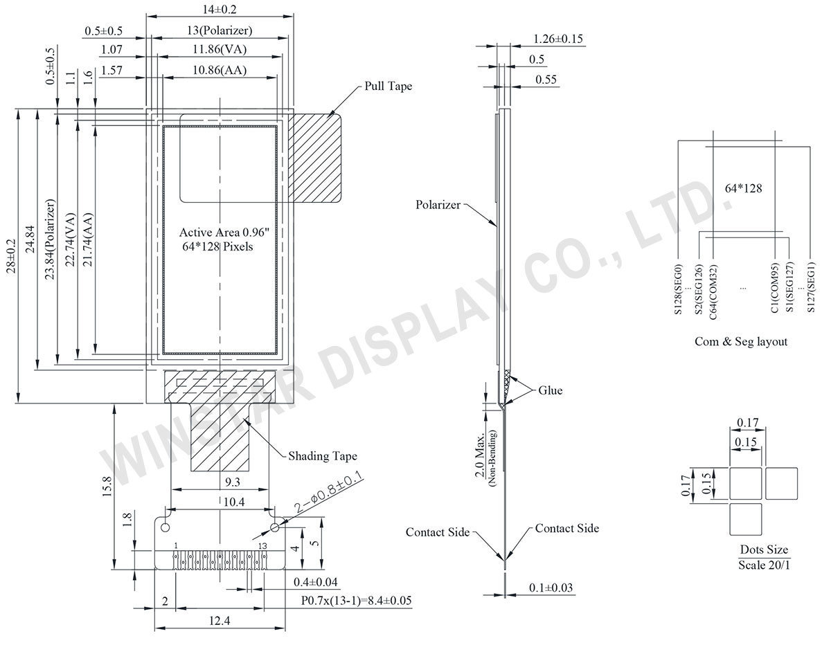
WEO064128A 型号是一款消费级 图形型 COG OLED 显示屏,对角线尺寸为 0.96 英寸,分辨率为 64x128 像素。此64x128 OLED 显示屏内置SH1107 IC,并支持 4 线 SPI 和 I2C 两种接口。逻辑电压为 3V,显示器电压为 9V。显示 50% 棋盘图案时,电流为 8mA @ 9V VCC(典型值),驱动方式为 1/64。
WEO064128A 型号,搭载SH1107 OLED 显示屏,分辨率为 64x128,非常适合应用于穿戴设备、便携设备、智能医疗产品、个人健康守护设备、测量仪器、智能家居等领域。其工作温度范围为 -30℃ 至 +70℃,存储温度范围为 -30℃ 至 +70℃,因此适用于各种环境条件。
| 项目 | 规格 | 单位 |
|---|---|---|
| 点阵(分辨率) | 64 x 128 | Dots |
| 模块尺寸 | 14.0 × 28.0 × 1.26 | mm |
| 有效区域 | 10.86× 21.74 | mm |
| 像素大小 | 0.15 × 0.15 | mm |
| 像素间距 | 0.17 × 0.17 | mm |
| 显示模式 | 被动矩阵 | |
| 发光颜色 | 单色 | |
| 驱动方式 | 1/64 Duty | |
| IC | SH1107 | |
| 界面 | 4-线 SPI , I2C | |
| 尺寸 | 0.96 寸 | |
| 参数 | 符号 | 最小值 | 最大值 | 单位 |
|---|---|---|---|---|
| 逻辑电源电压 | VDD | -0.3 | 3.6 | V |
| 显示电源电压 | VPP | -0.3 | 17.0 | V |
| 工作温度 | TOP | -30 | +70 | °C |
| 储存温度 | TSTG | -30 | +70 | °C |
| 项目 | 符号 | 条件 | 最小值 | 典型值 | 最大值 | 单位 |
|---|---|---|---|---|---|---|
| 逻辑电源电压 | VDD | - | 1.65 | 3.0 | 3.3 | V |
| 显示电源电压 | VPP | - | 7.0 | 9.0 | 9.5 | V |
| 输入高电压 | VIH | - | 0.8×VDD | - | VDD | V |
| 输入低电压 | VIL | - | 0 | - | 0.2×VDD | V |
| 输出高电压 | VOH | - | 0.8×VDD | - | VDD | V |
| 输出低电压 | VOL | - | 0 | - | 0.2×VDD | V |
| VCC工作电流 (50% 开启显示) | IPP | VPP=9V | - | 8 | 12 | mA |
| No. | 符号 | 说明 |
|---|---|---|
| 1 | NC | Not connected. |
| 2 | VPP | This is the most positive voltage supply pad of the chip. It should be supplied externally. |
| 3 | VCOMH | This is a pad for the voltage output high level for common signals. A capacitor should be connected between this pad and VSS. |
| 4 | VDD | Power supply for logic and input. |
| 5 | IM1 | These are the MPU interface mode select pads. IM1 connect to VDD is I2C interface. IM1 connect to GND is 4-wire SPI interface. |
| 6 | IREF | This is a segment current reference pad. A resistor should be connected between this pad and VSS. Set the current at 15.625uA. |
| 7 | CS | This pad is the chip select input. When CS = “L”, then the chip select becomes active, and data/command I/O is enabled. |
| 8 | RES | This is a reset signal input pad. When RES is set to “L”, the settings are initialized. The reset operation is performed by the RES signal level. |
| 9 | DC | This is the Data/Command control pad that determines whether the data bits are data or a command. DC = “H”: the inputs at D0 to D1 are treated as display data. DC = “L”: the inputs at D0 to D1 are transferred to the command registers. In I2C interface, this pad serves as SA0 to distinguish the different address of OLED driver. |
| 10 | D0 | When the serial interface is selected, then D0 serves as the serial clock input pad (SCL) and D1 serves as the serial data input pad (SI). When the I2C interface is selected, then D0 serves as the serial clock input pad (SCL) and D1 serves as the serial data input pad (SDA). |
| 11 | D1 | |
| 12 | VSS | Ground. |
| 13 | NC | Not connected. |

通过点击「允许所有 Cookie」,代表您同意在您的设备上存储 Cookie 以增强网站浏览体验、分析网站使用情况并协助我们的营销和网站效能优化工作。您可以在我们的隐私权政策中找到有关于此的更多信息。