我们重视您的隐私
通过点击「允许所有 Cookie」,代表您同意在您的设备上存储 Cookie 以增强网站浏览体验、分析网站使用情况并协助我们的营销和网站效能优化工作。您可以在我们的隐私权政策中找到有关于此的更多信息。


| 项目 | 规格 | 单位 |
|---|---|---|
| 显示尺寸(对角线) | 2.8 | 寸 |
| 点阵(分辨率) | 240 x RGB x 320(TFT) | dots |
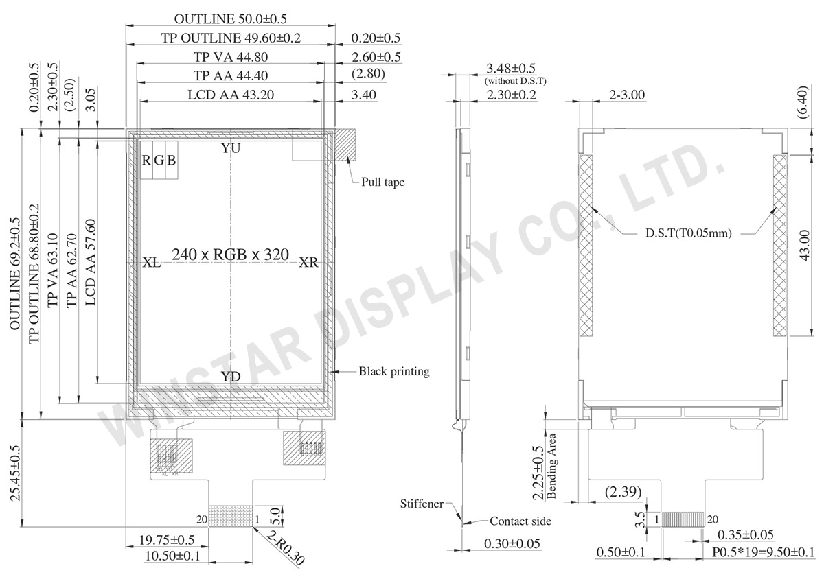
| 模块尺寸 | 50.0(W) x 69.2(H) x 3.48(D) | mm |
| 有效区域 | 43.2 x 57.6 | mm |
| 点间距 | 0.18 x 0.18 | mm |
| LCD 类型 | TFT, 白色, 透射式 | |
| 接口 | SPI | |
| TFT驱动IC | ST7789V或相容IC | |
| 视角 | 6点钟方向 | |
| 灰阶反转 | 12点钟方向 | |
| 长宽比 | 直屏 | |
| 背光类型 | LED, 白色 | |
| 触控面板类型 | RTP 电阻式触控面板 | |
| 表面 | 亮面 | |
| 项目 | 符号 | 最小值 | 典型值 | 最大值 | 单位 |
|---|---|---|---|---|---|
| 工作温度 | TOP | -20 | - | +70 | ℃ |
| 储存温度 | TST | -30 | - | +80 | ℃ |
| 项目 | 符号 | 最小值 | 典型值 | 最大值 | 单位 |
|---|---|---|---|---|---|
| 模拟电源电压 | Vcc | 2.4 | 3.3 | 3.6 | V |
| LCM供电电流 | Icc | - | 6.7 | 10.0 | mA |
| NO | 符号 | 功能说明 | ||||||||||||||||||
|---|---|---|---|---|---|---|---|---|---|---|---|---|---|---|---|---|---|---|---|---|
| 1 | GND | Ground | ||||||||||||||||||
| 2 | VLED+ | Anode of LED backlight. | ||||||||||||||||||
| 3 | VLED- | Cathode of LED backlight. | ||||||||||||||||||
| 4 | GND | Ground | ||||||||||||||||||
| 5 | VCC | Power supply | ||||||||||||||||||
| 6 | RESET | System reset pin. (RESX) signal is active low |
||||||||||||||||||
| 7 | SDA | When IM3: Low, SPI interface input/output pin. When IM3: High, SPI interface input pin. The data is latched on the rising edge of the SCL signal. If not used, please fix this pin at VDDI or DGND level. |
||||||||||||||||||
| 8 | DCX(SCL) | This pin is used to be serial interface clock. DCX=’1’: display data or parameter. DCX=’0’: command data. If not used, please fix this pin at VDDI or DGND. |
||||||||||||||||||
| 9 | CSX | Chip selection pin Low enable. High disable. |
||||||||||||||||||
| 10 | WRX(D/CX) | Display data/command selection pin in 4-line serial interface. Second Data lane in 2 data lane serial interface. If not used, please fix this pin at VDDI or DGND. |
||||||||||||||||||
| 11 | GND | Ground | ||||||||||||||||||
| 12 | SDO(DOUT) | SPI interface output pin. The data is output on the falling edge of the SCL signal. If not used, let this pin open. |
||||||||||||||||||
| 13 | TE | Tearing effect signal is used to synchronize MCU to frame memory writing. If not used, please let this pin open |
||||||||||||||||||
| 14 | IM3 | The MCU interface mode select.
|
||||||||||||||||||
| 15 | GND | Ground | ||||||||||||||||||
| 16 | XR | Right electrode | ||||||||||||||||||
| 17 | YD | Bottom electrode | ||||||||||||||||||
| 18 | XL | Left electrode | ||||||||||||||||||
| 19 | YU | Top electrode | ||||||||||||||||||
| 20 | GND | Ground |

通过点击「允许所有 Cookie」,代表您同意在您的设备上存储 Cookie 以增强网站浏览体验、分析网站使用情况并协助我们的营销和网站效能优化工作。您可以在我们的隐私权政策中找到有关于此的更多信息。