我们重视您的隐私
通过点击「允许所有 Cookie」,代表您同意在您的设备上存储 Cookie 以增强网站浏览体验、分析网站使用情况并协助我们的营销和网站效能优化工作。您可以在我们的隐私权政策中找到有关于此的更多信息。

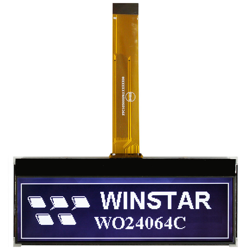
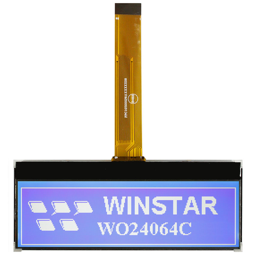
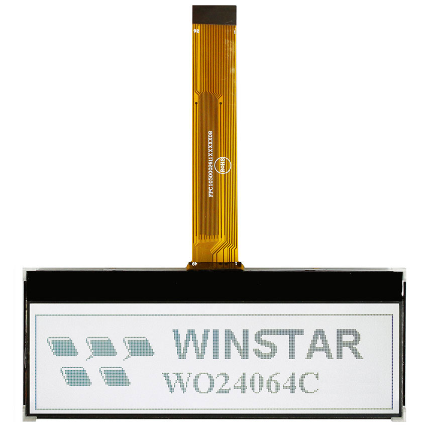
WO24064C 是一款 4.2 英寸 240x64 点阵 LCD 液晶显示屏,采用单色 COG 结构,搭载 ST7586S 控制器,支持 6800、8080、3-Line SPI 和 4-Line SPI 接口,采用 3.3V 逻辑电源。
模块尺寸为 111.0 x 58.0 x 13.6 mm,显示区域为 106.2 x 31.2 mm,有效显示区域为 103.17 x 27.49 mm,配备 LED 背光。同时提供多种 LCD 类型及 LED 背光组合可供选择,如有定制需求,请点击上方 『产品询价』,并在询价内容中说明您的规格要求。
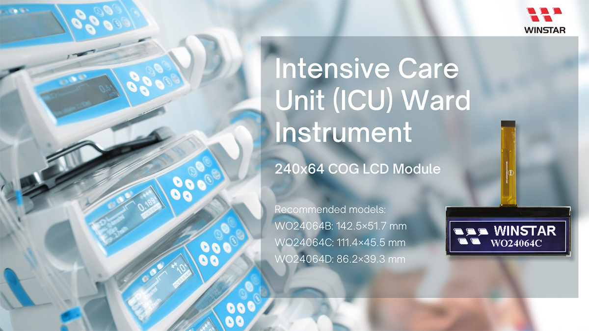
WO24064C 在保持 240x64 图形显示的同时,具备紧凑的模块尺寸,适用于医疗设备、生理监护设备、工业控制设备、测试测量仪器及各类嵌入式 HMI 应用。
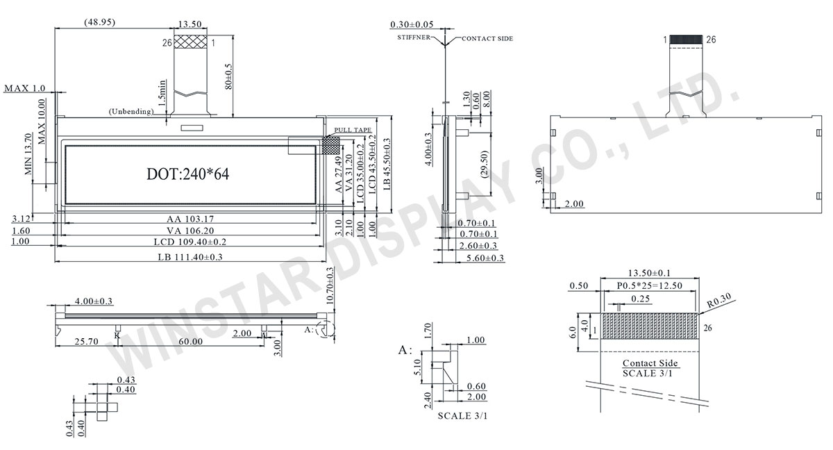
| 项目 | 标准尺寸 | 单位 |
|---|---|---|
| 点阵数 | 240 x 64 | - |
| 模块尺寸 | 111.0 x 58.0 x 13.6 (MAX) | mm |
| 检视区域 | 106.2 x 31.2 | mm |
| 有效区域 | 103.17 x 27.49 | mm |
| 点大小 | 0.40 x 0.40 | mm |
| 点间距 | 0.43 x 0.43 | mm |
| 驱动方式 | 1/64 | |
| 背光类型 | LED | |
| IC | ST7586S | |
| 接口 | 6800/8080/3-Line/4-Line | |
| 项目 | 符号 | 最小值 | 典型值 | 最大值 | 单位 |
|---|---|---|---|---|---|
| 工作温度 | TOP | -20 | - | +70 | ℃ |
| 储存温度 | TST | -30 | - | +80 | ℃ |
| LCD数位电源电压 | VDDI | -0.3 | - | 3.6 | V |
| 类比电源电压 | VDDA | -0.3 | - | 3.6 | V |
| LCD供电电压 | V0-XV0 | 0.3 | - | 19 | V |
| LCD供电电压 | VG | 0.3 | - | 5.5 | V |
| 项目 | 符号 | 条件 | 最小值 | 典型值 | 最大值 | 单位 |
|---|---|---|---|---|---|---|
| 逻辑电源电压 | VDD-VSS | - | 4.5 | 5.0 | 5.5 | V |
| LCM电源电压 | VDD-V0 | Ta=-20℃ Ta=25℃ Ta=70℃ |
- |
- 4.2 - |
- 4.5 - |
V V V |
| 输入高电压 | VIH | - | 2.5 | - | VDD | V |
| 输入低电压 | VIL | - | -0.3 | - | 0.6 | V |
| 输出高电压 | VOH | - | 3.9 | - | VDD | V |
| 输出低电压 | VOL | - | - | - | 0.4 | V |
| 电源电流(不包括LED背光) | IDD | VDD=5.0V | - | 1.0 | - | mA |
| Pin No. | 符号 | I/O | 说明 | ||||||||||||||||||||
|---|---|---|---|---|---|---|---|---|---|---|---|---|---|---|---|---|---|---|---|---|---|---|---|
| 1 | VG | P | VG is the power of SEG-drivers. | ||||||||||||||||||||
| 2 | XV0 | P | Negative operating voltage of COM-drivers. | ||||||||||||||||||||
| 3 | V0 | P | Positive operating voltage of COM-drivers. V0O is the output of the positive Vop generator. V0I is the positive Vop supply of LCD drivers. V0S is the sensor of the positive Vop generator. V0O, V0I & V0S should be separated on ITO and be connected together by FPC. |
||||||||||||||||||||
| 4 | VM | P | VM is the non-select voltage level of COM-drivers. | ||||||||||||||||||||
| 5 | VDDA | P | Analog power for internal booster | ||||||||||||||||||||
| 6 | VSS | P | Ground | ||||||||||||||||||||
| 7 | VD1 | P | VD1I is the power source of digital circuits. | ||||||||||||||||||||
| 8 | VDDI | P | Power of interface I/O circuit. | ||||||||||||||||||||
| 9 | CSB | Input | Chip select input pin. CSB=“L”: This chip is selected and the MPU interface is active. |
||||||||||||||||||||
| 10 | IF3 | Input | These pins select interface operation mode.
|
||||||||||||||||||||
| 11 | IF2 | ||||||||||||||||||||||
| 12 | IF1 | ||||||||||||||||||||||
| 13 | RSTB | Input | Reset input pin. When RSTB is “L”, internal initialization procedure is executed. | ||||||||||||||||||||
| 14 | /RD(E) | Input | Read / Write execution control pin. (This pin is only used in parallel interface) | ||||||||||||||||||||
| 15 | D7 | I/O | The bi-directional data bus of the MPU interface. When CSB is “H”, they are high impedance. If using serial interface: D0 is the SDA signal in 4-Line & 3-Line interface. D1 is the A0 signal in 4-Line interface |
||||||||||||||||||||
| 16 | D6 | ||||||||||||||||||||||
| 17 | D5 | ||||||||||||||||||||||
| 18 | D4 | ||||||||||||||||||||||
| 19 | D3 | ||||||||||||||||||||||
| 20 | D2 | ||||||||||||||||||||||
| 21 | D1 | ||||||||||||||||||||||
| 22 | D0 | ||||||||||||||||||||||
| 23 | NC | Input | No connection | ||||||||||||||||||||
| 24 | /WR(R/W) | Read / Write execution control pin. (This pin is only used in parallel interface) | |||||||||||||||||||||
| 25 | A0(SCL) | Input |
The function of this pin is different in parallel and serial interface. |
||||||||||||||||||||
| 26 | VSS | Input | Ground |


通过点击「允许所有 Cookie」,代表您同意在您的设备上存储 Cookie 以增强网站浏览体验、分析网站使用情况并协助我们的营销和网站效能优化工作。您可以在我们的隐私权政策中找到有关于此的更多信息。