우리는 귀하의 프라이버시를 소중히 여깁니다
"모든 쿠키 허용"을 클릭하면 사이트 탐색을 개선하고, 사이트 사용을 분석하며, 마케팅 및 성능 노력에 도움을 주기 위해 쿠키를 귀하의 장치에 저장하는 데 동의한 것으로 간주됩니다. 이 주제에 대한 추가 정보는 당사의 정책에서 확인할 수 있습니다. 개인정보 보호정책

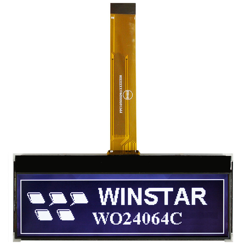
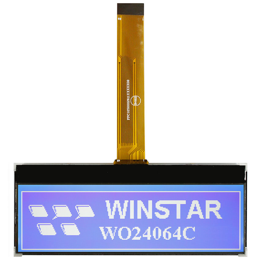
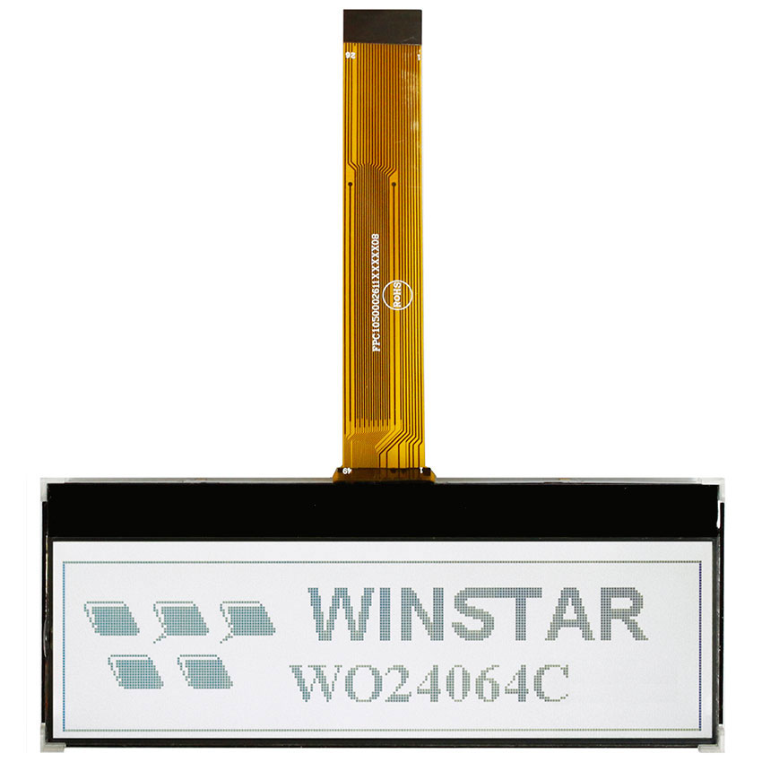
WO24064C는 4.2인치 240x64 도트 매트릭스 LCD 모듈로, 모노크롬 COG 구조와 ST7586S 컨트롤러를 탑재하고 6800, 8080, 3-Line SPI 및 4-Line SPI 인터페이스를 지원합니다. 로직 전원은 3.3V입니다.
모듈 크기는 111.0 x 58.0 x 13.6 mm이며, 표시 영역(VA)은 106.2 x 31.2 mm, 유효 표시 영역(AA)은 103.17 x 27.49 mm입니다. LED 백라이트를 적용했으며, 다양한 LCD 타입과 LED 백라이트 조합을 선택할 수 있습니다. 맞춤 사양이 필요한 경우 상단의 문의 추가를 클릭하여 요구 사항을 남겨주시기 바랍니다.
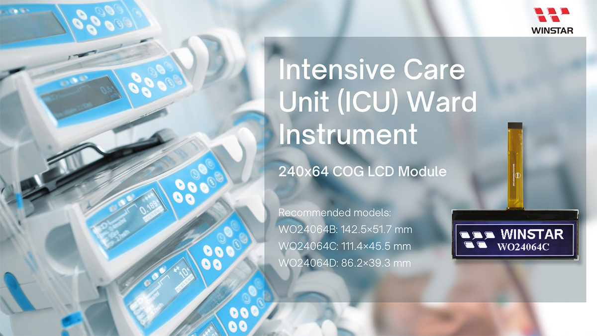
WO24064C는 240x64 그래픽 표시 성능을 유지하면서도 컴팩트한 크기를 제공하여 의료기기, 생체 모니터링 장비, 산업용 컨트롤러, 계측기 및 다양한 임베디드 HMI 애플리케이션에 적합합니다.
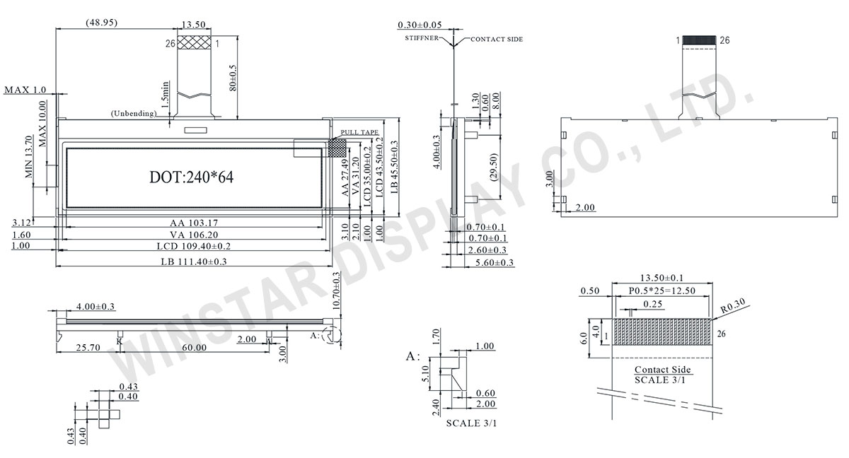
| 항목 | 치수 | 단위 |
|---|---|---|
| 표시 도트 수 | 240 x 64 | - |
| 모듈 치수 | 111.0 x 58.0 x 13.6 (MAX) | mm |
| 보기 영역 | 106.2 x 31.2 | mm |
| 활성 영역 | 103.17 x 27.49 | mm |
| 도트 크기 | 0.40 x 0.40 | mm |
| 도트 피치 | 0.43 x 0.43 | mm |
| 듀티 | 1/64 | |
| 역광 타입 | LED | |
| IC | ST7586S | |
| 인터페이스 | 6800/8080/3-Line/4-Line | |
| 항목 | 기호 | 최소값 | 대표값 | 최대값 | 단위 |
|---|---|---|---|---|---|
| 작동 온도 | TOP | -20 | - | +70 | ℃ |
| 보관 온도 | TST | -30 | - | +80 | ℃ |
| Digital Power Supply Voltage | VDDI | -0.3 | - | 3.6 | V |
| Analog Power supply voltage | VDDA | -0.3 | - | 3.6 | V |
| LCD Power supply voltage | V0-XV0 | 0.3 | - | 19 | V |
| LCD Power supply voltage | VG | 0.3 | - | 5.5 | V |
| 항목 | 기호 | 조건 | 최소값 | 대표값 | 최대값 | 단위 |
|---|---|---|---|---|---|---|
| Supply Voltage For Logic | VDD-VSS | - | 4.5 | 5.0 | 5.5 | V |
| Supply Voltage For LCM | VDD-V0 | Ta=-20℃ Ta=25℃ Ta=70℃ |
- |
- 4.2 - |
- 4.5 - |
V V V |
| Input High Volt. | VIH | - | 2.5 | - | VDD | V |
| Input Low Volt. | VIL | - | -0.3 | - | 0.6 | V |
| Output High Volt. | VOH | - | 3.9 | - | VDD | V |
| Output Low Volt. | VOL | - | - | - | 0.4 | V |
| Supply Current(No include LED Backlight) | IDD | VDD=5.0V | - | 1.0 | - | mA |
| Pin No. | 기호 | I/O | 설명 | ||||||||||||||||||||
|---|---|---|---|---|---|---|---|---|---|---|---|---|---|---|---|---|---|---|---|---|---|---|---|
| 1 | VG | P | VG is the power of SEG-drivers. | ||||||||||||||||||||
| 2 | XV0 | P | Negative operating voltage of COM-drivers. | ||||||||||||||||||||
| 3 | V0 | P | Positive operating voltage of COM-drivers. V0O is the output of the positive Vop generator. V0I is the positive Vop supply of LCD drivers. V0S is the sensor of the positive Vop generator. V0O, V0I & V0S should be separated on ITO and be connected together by FPC. |
||||||||||||||||||||
| 4 | VM | P | VM is the non-select voltage level of COM-drivers. | ||||||||||||||||||||
| 5 | VDDA | P | Analog power for internal booster | ||||||||||||||||||||
| 6 | VSS | P | Ground | ||||||||||||||||||||
| 7 | VD1 | P | VD1I is the power source of digital circuits. | ||||||||||||||||||||
| 8 | VDDI | P | Power of interface I/O circuit. | ||||||||||||||||||||
| 9 | CSB | Input | Chip select input pin. CSB=“L”: This chip is selected and the MPU interface is active. |
||||||||||||||||||||
| 10 | IF3 | Input | These pins select interface operation mode.
|
||||||||||||||||||||
| 11 | IF2 | ||||||||||||||||||||||
| 12 | IF1 | ||||||||||||||||||||||
| 13 | RSTB | Input | Reset input pin. When RSTB is “L”, internal initialization procedure is executed. | ||||||||||||||||||||
| 14 | /RD(E) | Input | Read / Write execution control pin. (This pin is only used in parallel interface) | ||||||||||||||||||||
| 15 | D7 | I/O | The bi-directional data bus of the MPU interface. When CSB is “H”, they are high impedance. If using serial interface: D0 is the SDA signal in 4-Line & 3-Line interface. D1 is the A0 signal in 4-Line interface |
||||||||||||||||||||
| 16 | D6 | ||||||||||||||||||||||
| 17 | D5 | ||||||||||||||||||||||
| 18 | D4 | ||||||||||||||||||||||
| 19 | D3 | ||||||||||||||||||||||
| 20 | D2 | ||||||||||||||||||||||
| 21 | D1 | ||||||||||||||||||||||
| 22 | D0 | ||||||||||||||||||||||
| 23 | NC | Input | No connection | ||||||||||||||||||||
| 24 | /WR(R/W) | Read / Write execution control pin. (This pin is only used in parallel interface) | |||||||||||||||||||||
| 25 | A0(SCL) | Input |
The function of this pin is different in parallel and serial interface. |
||||||||||||||||||||
| 26 | VSS | Input | Ground |


"모든 쿠키 허용"을 클릭하면 사이트 탐색을 개선하고, 사이트 사용을 분석하며, 마케팅 및 성능 노력에 도움을 주기 위해 쿠키를 귀하의 장치에 저장하는 데 동의한 것으로 간주됩니다. 이 주제에 대한 추가 정보는 당사의 정책에서 확인할 수 있습니다. 개인정보 보호정책