

私たちはあなたのプライバシーを大切にします
「すべてのクッキーを許可」をクリックすると、サイトのナビゲーションを向上させ、サイト使用状況を分析し、マーケティングおよびパフォーマンスの取り組みを支援するために、クッキーをデバイスに保存することに同意したことになります。この件に関する詳細情報は、ポリシーをご覧ください。プライバシーポリシー


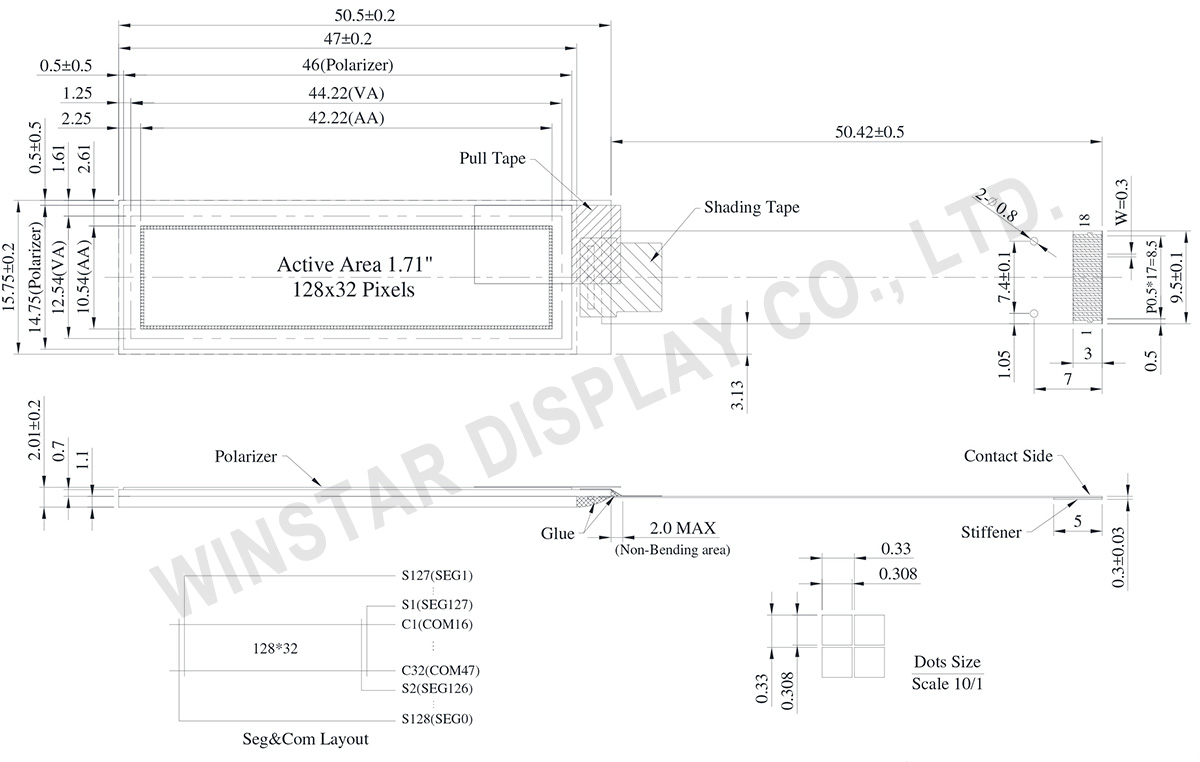
WEO012832Pは128x32ドットで構成された1.71インチのCOGモジュールです。CH1115 ICが組み込まれ、I2C および 4 線式 SPI インターフェース、3V ロジック電源電圧、1/32 駆動デューティをサポートいたします。50% チェッカーボード表示での電流は 5mA @ 12V VCC (白色の場合) です。
WEO012832PはWEO012832Gとは機械的サイズとPFC ピン定義は同じです。WEO012832PはCH1115 IC搭載品で、その詳細仕様については製品仕様書をご確認願います。
薄型、軽量、低消費電力というメリットを備えたWEO012832Pは携帯機器、健康機器、検査機器などに適しております。その動作温度範囲は-40℃ ~ +80℃で、保管温度範囲は-40℃~+85℃です。
| 項目 | 仕様 | 単位 |
|---|---|---|
| 解像度 | 128 × 32 | Dots |
| 外形寸法 | 50.50 × 15.75 × 2.01 | mm |
| 有効エリア | 42.22 × 10.54 | mm |
| ドットサイズ | 0.308 × 0.308 | mm |
| ドットピッチ | 0.33 × 0.33 | mm |
| 表示モード | パッシブマトリクス | |
| 発光色 | モノクロ | |
| 駆動方法 | 1/32 Duty | |
| IC | CH1115 | |
| インターフェイス | SPI, I2C | |
| サイズ | 1.71 インチ | |
| パラメーター | 記号 | 最小値 | 最大値 | 単位 |
|---|---|---|---|---|
| ロジック電源電圧 | VDD | -0.3 | 3.6 | V |
| Display電源電圧 | VPP | -0.3 | 14.5 | V |
| 操作温度 | TOP | -40 | +80 | °C |
| 保存温度 | TSTG | -40 | +85 | °C |
| 項目 | 記号 | 条件 | 最小値 | 典型値 | 最大値 | 単位 |
|---|---|---|---|---|---|---|
| ロジック電源電圧 | VDD | - | 1.65 | 3.0 | 3.3 | V |
| Display電源電圧 | VPP | - | 6.4 | 12.0 | 12.5 | V |
| 高レベル入力 | VIH | - | 0.8×VDD | - | VDD | V |
| 低レベル入力 | VIL | - | VSS | - | 0.2×VDD | V |
| 高レベル出力 | VOH | - | 0.8×VDD | - | VDD | V |
| 低レベル出力 | VOL | - | VSS | - | 0.2×VDD | V |
| Display 50% Pixel on | IPP | VPP=12V | - | 5 | 10 | mA |
| No. | 記号 | 説明 | ||||||||||||
|---|---|---|---|---|---|---|---|---|---|---|---|---|---|---|
| 1 | ESD_GND | ESD Ground pin | ||||||||||||
| 2 | VPP | OLED panel power supply. | ||||||||||||
| 3 | VSS | This is a ground pin. | ||||||||||||
| 4 | VSS | This is a ground pin. | ||||||||||||
| 5 | VDD | Power Supply for Logic | ||||||||||||
| 6 | __ CS |
This pad is the chip select input. When /CS = “L”, then the chip select becomes active, and data/command I/O is enabled. | ||||||||||||
| 7 | ___ RES |
This is a reset signal input pad. When /RES is set to “L”, the settings are initialized. The reset operation is performed by the /RES signal level. | ||||||||||||
| 8 | A0 | This is the Data/Command control pad that determines whether the data bits are data or a command. In I2C interface, this pad serves as SA0 to distinguish the different address of OLED driver. |
||||||||||||
| 9 | SCL | The serial clock input pad | ||||||||||||
| 10 | SI/SDA | The serial data input pad | ||||||||||||
| 11 | NC | Dummy Pin | ||||||||||||
| 12 | IREF | This is a segment current reference pad. A resistor should be connected between this pad and VSS. Set the current at 18.75μA. | ||||||||||||
| 13 | VCOMH | The pin is for COM signal deselected voltage level. A capacitor should be connected between this pin and VSS. |
||||||||||||
| 14 | VPP | OLED panel power supply. | ||||||||||||
| 15 | IM0 | These are the MPU interface mode select pads.
|
||||||||||||
| 16 | IM1 | |||||||||||||
| 17 | VSS | This is a ground pin. | ||||||||||||
| 18 | ESD_GND | ESD Ground pin |

「すべてのクッキーを許可」をクリックすると、サイトのナビゲーションを向上させ、サイト使用状況を分析し、マーケティングおよびパフォーマンスの取り組みを支援するために、クッキーをデバイスに保存することに同意したことになります。この件に関する詳細情報は、ポリシーをご覧ください。プライバシーポリシー