
我们重视您的隐私
通过点击「允许所有 Cookie」,代表您同意在您的设备上存储 Cookie 以增强网站浏览体验、分析网站使用情况并协助我们的营销和网站效能优化工作。您可以在我们的隐私权政策中找到有关于此的更多信息。


WEO012832P是一款对角线为1.71寸COG图形OLED显示器模块,显示画面由128x32像素组成。此模块电源电压典型值为 3V (VDD),内建采用CH1115 IC,可支持I2C、SPI接口,驱动方式1/32 duty;50%棋盘格显示电流为20mA @ VCC 12V (白色)。
WEO012832P 这款模块型号是WEO012832G模块的IC替代解决方案,机构尺寸及FPC出PIN定义两款均相同。此款模块是COG结构OLED显示屏,超薄、无需背光源,模块重量轻,功耗低,节能减碳。
适用于智能家电产品、携带型装置、智能医疗产品、量测仪器等产品;模块的工作温度是-40℃至+80℃,储存温度-40℃至+85℃。
| 项目 | 尺寸 | 单位 |
|---|---|---|
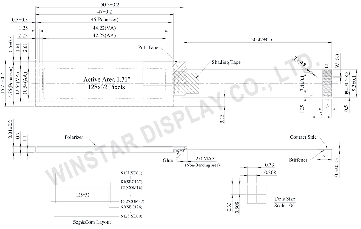
| 分辨率 | 128 × 32 | Dots |
| 模块尺寸 | 50.50 × 15.75 × 2.01 | mm |
| 检视区域 | 42.22 × 10.54 | mm |
| 点大小 | 0.308 × 0.308 | mm |
| 点间距 | 0.33 × 0.33 | mm |
| 显示模式 | 被动矩阵 | |
| 发光颜色 | 单色 | |
| 驱动方式 | 1/32 Duty | |
| IC | CH1115 | |
| 接口 | SPI, I2C | |
| 尺寸 | 1.71 寸 | |
| 参数 | 符号 | 最小值 | 最大值 | 单位 |
|---|---|---|---|---|
| 逻辑电源电压 | VDD | -0.3 | 3.6 | V |
| 显示电源电压 | VPP | -0.3 | 14.5 | V |
| 工作温度 | TOP | -40 | +80 | °C |
| 储存温度 | TSTG | -40 | +85 | °C |
| 项目 | 符号 | 条件 | 最小值 | 标准值 | 最大值 | 单位 |
|---|---|---|---|---|---|---|
| 逻辑电源电压 | VDD | - | 1.65 | 3.0 | 3.3 | V |
| 显示电源电压 | VPP | - | 6.4 | 12.0 | 12.5 | V |
| 输入高准位 | VIH | - | 0.8×VDD | - | VDD | V |
| 输入低准位 | VIL | - | VSS | - | 0.2×VDD | V |
| 输出高准位 | VOH | - | 0.8×VDD | - | VDD | V |
| 输出低准位 | VOL | - | VSS | - | 0.2×VDD | V |
| Display 50% Pixel on | IPP | VPP=12V | - | 5 | 10 | mA |
| No. | 符号 | 功能说明 | ||||||||||||
|---|---|---|---|---|---|---|---|---|---|---|---|---|---|---|
| 1 | ESD_GND | ESD Ground pin | ||||||||||||
| 2 | VPP | OLED panel power supply. | ||||||||||||
| 3 | VSS | This is a ground pin. | ||||||||||||
| 4 | VSS | This is a ground pin. | ||||||||||||
| 5 | VDD | Power Supply for Logic | ||||||||||||
| 6 | __ CS |
This pad is the chip select input. When /CS = “L”, then the chip select becomes active, and data/command I/O is enabled. | ||||||||||||
| 7 | ___ RES |
This is a reset signal input pad. When /RES is set to “L”, the settings are initialized. The reset operation is performed by the /RES signal level. | ||||||||||||
| 8 | A0 | This is the Data/Command control pad that determines whether the data bits are data or a command. In I2C interface, this pad serves as SA0 to distinguish the different address of OLED driver. |
||||||||||||
| 9 | SCL | The serial clock input pad | ||||||||||||
| 10 | SI/SDA | The serial data input pad | ||||||||||||
| 11 | NC | Dummy Pin | ||||||||||||
| 12 | IREF | This is a segment current reference pad. A resistor should be connected between this pad and VSS. Set the current at 18.75μA. | ||||||||||||
| 13 | VCOMH | The pin is for COM signal deselected voltage level. A capacitor should be connected between this pin and VSS. |
||||||||||||
| 14 | VPP | OLED panel power supply. | ||||||||||||
| 15 | IM0 | These are the MPU interface mode select pads.
|
||||||||||||
| 16 | IM1 | |||||||||||||
| 17 | VSS | This is a ground pin. | ||||||||||||
| 18 | ESD_GND | ESD Ground pin |

通过点击「允许所有 Cookie」,代表您同意在您的设备上存储 Cookie 以增强网站浏览体验、分析网站使用情况并协助我们的营销和网站效能优化工作。您可以在我们的隐私权政策中找到有关于此的更多信息。