
우리는 귀하의 프라이버시를 소중히 여깁니다
"모든 쿠키 허용"을 클릭하면 사이트 탐색을 개선하고, 사이트 사용을 분석하며, 마케팅 및 성능 노력에 도움을 주기 위해 쿠키를 귀하의 장치에 저장하는 데 동의한 것으로 간주됩니다. 이 주제에 대한 추가 정보는 당사의 정책에서 확인할 수 있습니다. 개인정보 보호정책


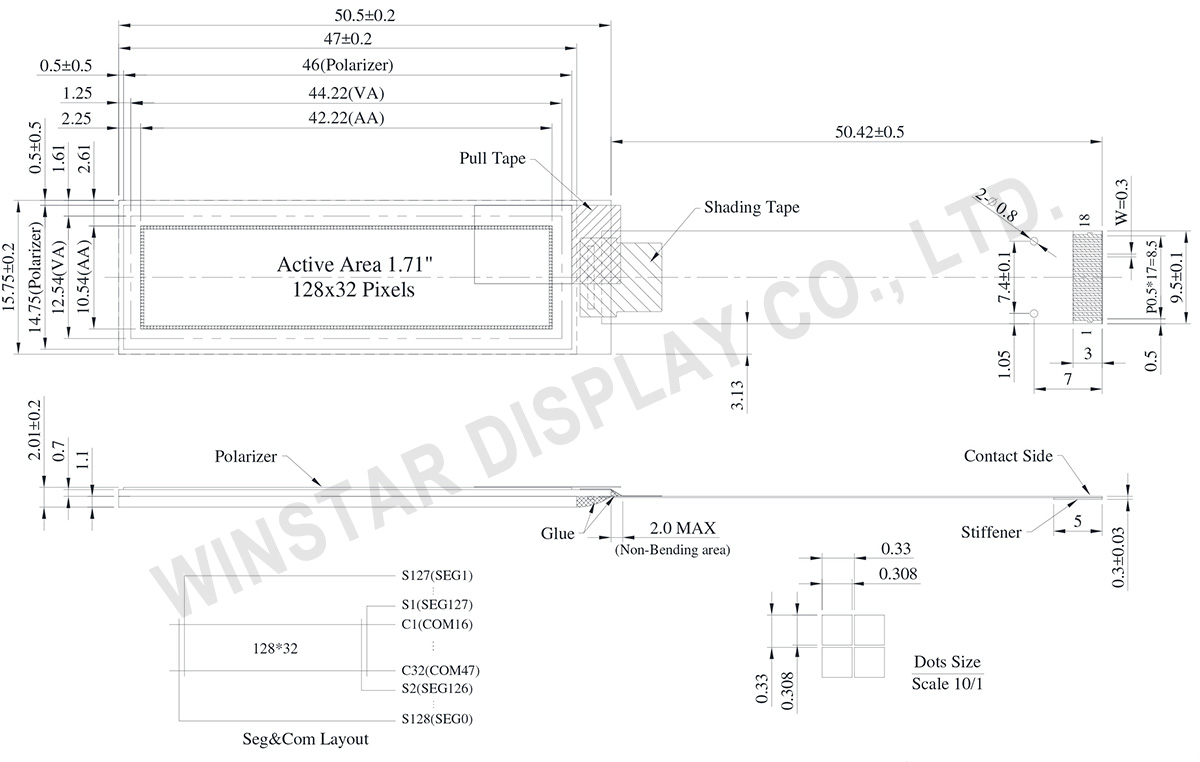
이 WEO012832P 제품은 COG OLED 디스플레이로 128x32 도트로 구성되어 있으며, 대각선 길이는 1,71인치입니다. 이 모듈의 모듈 크기는 50.50x15.75 mm이며 활성 영역 면적은 42.22x10.54 mm입니다. 이 모듈은 CH1115 IC가 기본 내장되어 있으며 I2C 및 SPI 인터페이스를 지원합니다.
논리 공급 전압은 1.65V에서 3.3V, 일반값 3V이며 디스플레이 공급 전압은 12V, 1/32 (구동 부하)입니다. 이 모듈 시리즈의 작동 온도는 -40℃에서 +80℃이며, 보관 온도 범위는 -40℃에서 +85℃입니다.
| 항목 | 치수 | 단위 |
|---|---|---|
| 도트 매트릭스 | 128 × 32 | Dots |
| 모듈 치수 | 50.50 × 15.75 × 2.01 | mm |
| 활성 영역 | 42.22 × 10.54 | mm |
| 도트 크기 | 0.308 × 0.308 | mm |
| 도트 피치 | 0.33 × 0.33 | mm |
| 디스플레이 모드 | 패시브 매트릭스 | |
| 디스플레이 색상 | Monochrome | |
| Drive Duty | 1/32 Duty | |
| IC | CH1115 | |
| 인터페이스 | SPI, I2C | |
| 크기 | 1.71 인치 | |
| Parameter | 기호 | 최소값 | 최대값 | 단위 |
|---|---|---|---|---|
| Supply Voltage for Logic | VDD | -0.3 | 3.6 | V |
| Supply Voltage for Display | VPP | -0.3 | 14.5 | V |
| 작동 온도 | TOP | -40 | +80 | °C |
| 보관 온도 | TSTG | -40 | +85 | °C |
| 항목 | 기호 | 조건 | 최소값 | 대표값 | 최대값 | 단위 |
|---|---|---|---|---|---|---|
| Supply Voltage for Logic | VDD | - | 1.65 | 3.0 | 3.3 | V |
| Supply Voltage for Display | VPP | - | 6.4 | 12.0 | 12.5 | V |
| High Level Input | VIH | - | 0.8×VDD | - | VDD | V |
| Low Level Input | VIL | - | VSS | - | 0.2×VDD | V |
| High Level Output | VOH | - | 0.8×VDD | - | VDD | V |
| Low Level Output | VOL | - | VSS | - | 0.2×VDD | V |
| Display 50% Pixel on | IPP | VPP=12V | - | 5 | 10 | mA |
| No. | 기호 | 기능 | ||||||||||||
|---|---|---|---|---|---|---|---|---|---|---|---|---|---|---|
| 1 | ESD_GND | ESD Ground pin | ||||||||||||
| 2 | VPP | OLED panel power supply. | ||||||||||||
| 3 | VSS | This is a ground pin. | ||||||||||||
| 4 | VSS | This is a ground pin. | ||||||||||||
| 5 | VDD | Power Supply for Logic | ||||||||||||
| 6 | __ CS |
This pad is the chip select input. When /CS = “L”, then the chip select becomes active, and data/command I/O is enabled. | ||||||||||||
| 7 | ___ RES |
This is a reset signal input pad. When /RES is set to “L”, the settings are initialized. The reset operation is performed by the /RES signal level. | ||||||||||||
| 8 | A0 | This is the Data/Command control pad that determines whether the data bits are data or a command. In I2C interface, this pad serves as SA0 to distinguish the different address of OLED driver. |
||||||||||||
| 9 | SCL | The serial clock input pad | ||||||||||||
| 10 | SI/SDA | The serial data input pad | ||||||||||||
| 11 | NC | Dummy Pin | ||||||||||||
| 12 | IREF | This is a segment current reference pad. A resistor should be connected between this pad and VSS. Set the current at 18.75μA. | ||||||||||||
| 13 | VCOMH | The pin is for COM signal deselected voltage level. A capacitor should be connected between this pin and VSS. |
||||||||||||
| 14 | VPP | OLED panel power supply. | ||||||||||||
| 15 | IM0 | These are the MPU interface mode select pads.
|
||||||||||||
| 16 | IM1 | |||||||||||||
| 17 | VSS | This is a ground pin. | ||||||||||||
| 18 | ESD_GND | ESD Ground pin |

"모든 쿠키 허용"을 클릭하면 사이트 탐색을 개선하고, 사이트 사용을 분석하며, 마케팅 및 성능 노력에 도움을 주기 위해 쿠키를 귀하의 장치에 저장하는 데 동의한 것으로 간주됩니다. 이 주제에 대한 추가 정보는 당사의 정책에서 확인할 수 있습니다. 개인정보 보호정책