 - WF0128BTYAA4DNN0")

我們重視您的隱私
通過點擊「允許所有 Cookie」,代表您同意在您的設備上存儲 Cookie 以增強網站瀏覽體驗、分析網站使用情況並協助我們的行銷和網站效能優化工作。您可以在我們的隱私權政策中找到有關於此的更多資訊。


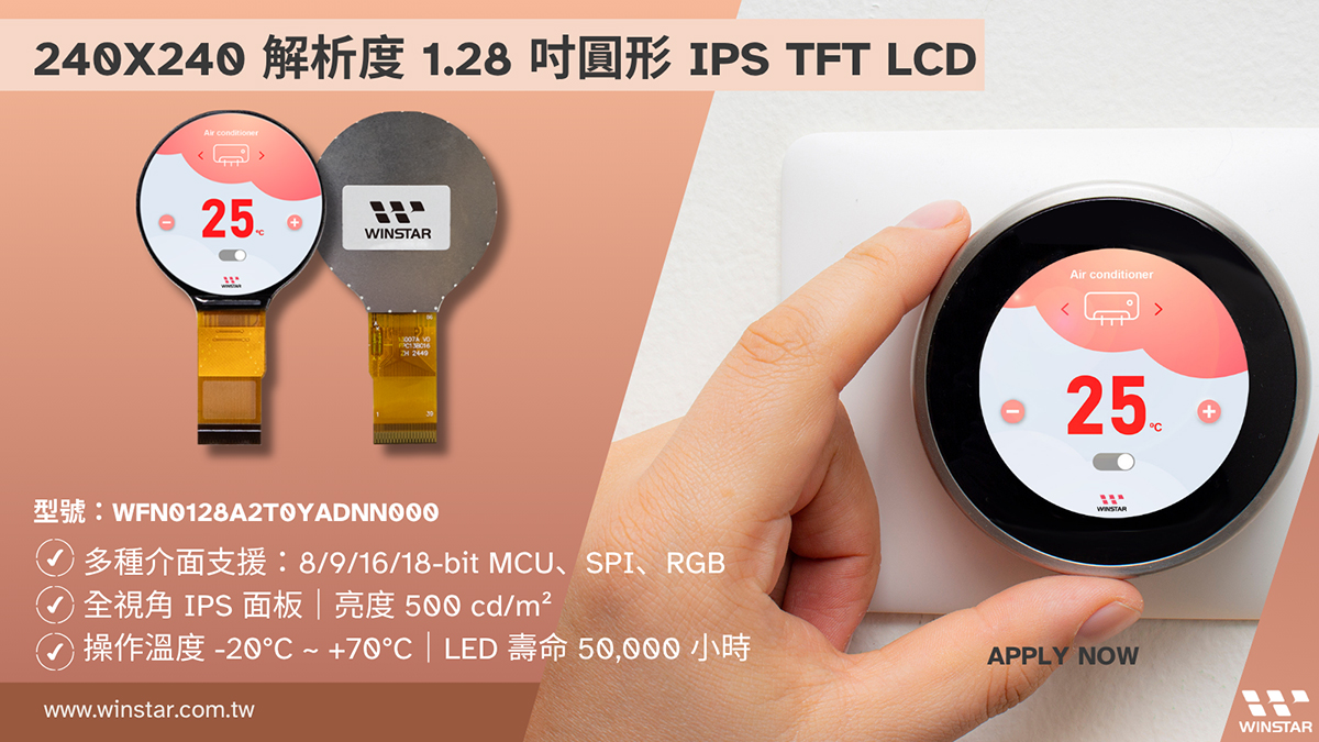
GC9A01 1.28吋 TFT圓形LCD模組提供高解析度240x240 IPS視覺效果,是需要圓形顯示器應用的理想選擇。此模組專為嚴苛環境設計,具備卓越的性能、長效耐用性,並可輕鬆整合至各種系統中。
搭載GC9A01驅動IC,該模組支持多種彈性的接口選項,包括8/9/16/18位元MCU、3/4線SPI串行接口以及16/18位元RGB,確保與各種主控平台的兼容性。亮度高達500 cd/m²,對比度達700:1,即使在不同光照條件下也能穩定顯示。此外,該模組具備從-20℃至+70℃的廣泛工作溫度範圍,並且LED壽命長達50,000小時,提供可靠且具成本效益的長期解決方案。
GC9A01 1.28吋 TFT圓形LCD顯示模組是需要緊湊且高效能圓形顯示的應用理想選擇。憑藉其靈活的接口選項、廣泛的工作溫度範圍和長效的運行壽命,旨在滿足工業和消費級設備的需求。
| 項目 | 規格 | 單位 |
|---|---|---|
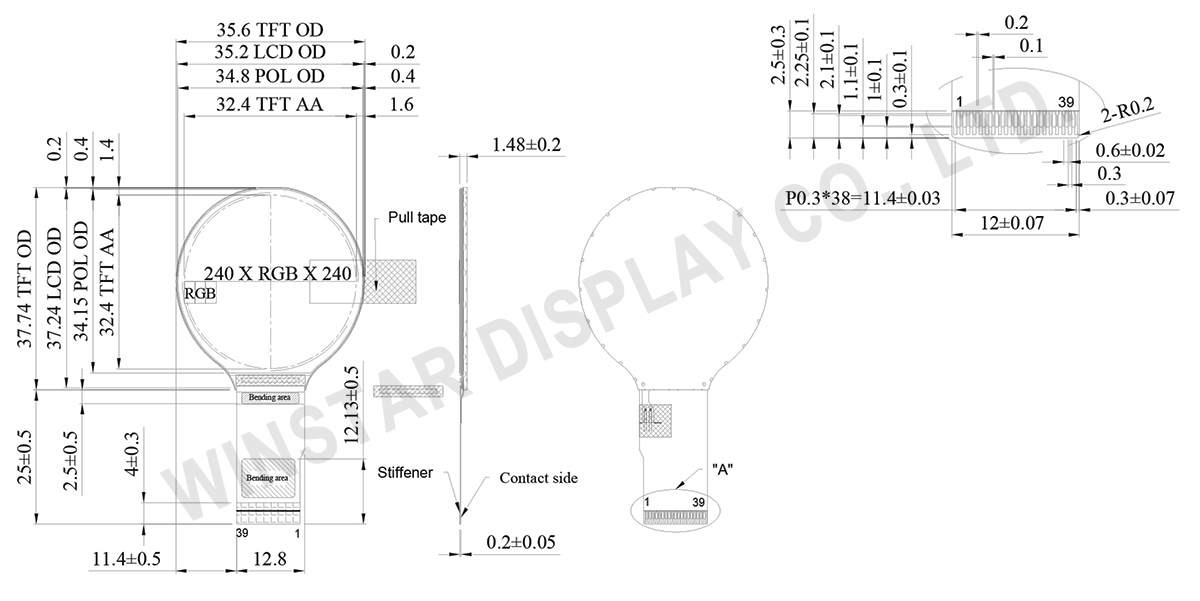
| 尺寸(對角線) | 1.28 | 吋 |
| 點陣(解析度) | 240 × RGB × 240 (TFT) | dots |
| 模組尺寸 | 35.6 × 37.74 × 1.48 | mm |
| 有效區域 | 32.4 × 32.4 | mm |
| 像素間距 | 0.135 × 0.135 | mm |
| LCD類型 | TFT全透 | |
| 視角 | 85/85/85/85 | |
| TFT 介面 | 8/9/16/18bit MCU 3/4SPI+16/18BIT RGB 3/4 Serial |
|
| 背光類型 | LED, 白色 | |
| 驅動IC | GC9A01 | |
| 觸控面板 | 無觸控面板 | |
| 表面 | 防眩光 | |
| 項目 | 符號 | 最小值 | 典型值 | 最大值 | 單位 |
|---|---|---|---|---|---|
| 工作溫度 | TOP | -20 | - | +70 | ℃ |
| 儲存溫度 | TST | -30 | - | +80 | ℃ |
| 項目 | 符號 | 最小值 | 典型值 | 最大值 | 單位 |
|---|---|---|---|---|---|
| 數位供電電壓 | VCC | 2.5 | 2.8 | 3.3 | V |
| 數位介面供電電壓 | IOVCC | 1.65 | 2.8 | 3.3 | V |
| 正常模式電流消耗 | ICC | -- | 6 | 12 | mA |
| 輸入電壓範圍 | VIH | 0.7*IOVCC | -- | IOVCC | V |
| VIL | GND | -- | 0.3*IOVCC | V | |
| 輸出電壓範圍 | VOH | 0.8*IOVCC | -- | IOVCC | V |
| VOL | GND | -- | 0.2*IOVCC | V |
| 項目 | 符號 | 最小值 | 典型值 | 最大值 | 單位 |
|---|---|---|---|---|---|
| LED電流 | - | - | 40 | - | mA |
| LED電壓 | VLED+ | 2.8 | 3.0 | 3.2 | V |
| LED使用壽命 | - | 50000 | - | - | Hr |
| Pin No | 符號 | 功能說明 | I/O |
|---|---|---|---|
| 1 | VLED+ | Anode pin of backlight | P |
| 2 | VLED* | Cathode pin of backlight | P |
| 3 | GND | Ground. | P |
| 4 | GND | Ground. | P |
| 5 | VCC | Supply voltage (2.5-3.3V). | P |
| 6 | IOVCC | Supply voltage (1.65-3.3V). | P |
| 7 | RESET | This signal will reset the device and must be applied to properly initialize the chip. |
I |
| 8 | WR(SPI-RS) | -Write enable in MCU parallel interface. Display data/command selection pin in 4-line serial interface. Second Data lane in 2 data lane serial interface. -If not used, please fix this pin at IOVCC or GND. |
I |
| 9 | CS | Chip select input pin (“Low” enable ,CSX). Fix this pin at IOVCC or GND when not in use. |
I |
| 10 | RS(SPI-SCL) | -Display data/command selection pin in parallel interface.(D/CX) -This pin is used to be serial interface clock. (SCL) DC=’1’: display data or parameter. DC=’0’: command data. -If not used, please fix this pin at IOVCC or GND. |
I |
| 11 | RD | Serves as a read signal and MCU read data at the rising edge. Fix this pin at IOVCC or GND when not in use. |
I |
| 12 | PCLK | Dot clock signal for RGB interface operation. (DOTCLK) Fix this pin at IOVCC or GND when not in use. |
I |
| 13 | DE | Data enable signal for RGB interface operation. (ENABLE) fix this pin at IOVCC or GND when not in use. |
I |
| 14 | VSYNC | Frame synchronizing signal for RGB interface operation. fix this pin at IOVCC or GND when not in use. |
I |
| 15 | HSYNC | Line synchronizing signal for RGB interface operation. fix this pin at IOVCC or GND when not in use. |
I |
| 16 | TE | Tearing effect output pin to synchronize MPU to frame writing, activated by S/W command. When this pin is not activated, this pin is low. If not used, open this pin. |
I |
| 17 | NC | No connection | O |
| 18 | SDA | The data is latched on the rising edge of the SCL signal. If not used, please fix this pin at IOVCC or GND level |
I/O |
| 19-36 | DB17-DB0 | 18-bit parallel bi-directional data bus for MCU system and RGB interface mode . 18-bit RGB DB0:BLUE LSB--DB5:BLUE MSB; DB6:GREEN LSB--DB11:GREEN,MSB; DB12:RED LSB--DB17:RED MSB. 16-bit RGB: DB1:BLUE LSB--DB5:BLUE MSB; DB6:GREEN LSB--DB11:GREEN,MSB; DB13:RED LSB--DB17:RED MSB. mode Fix to GND level when not in use |
I/O |
| 37 | IM0 | MPU Parallel interface bus and serial interface select If use RGB Interface must select serial interface. Fix this pin at IOVCC and GND. |
I |
| 38 | IM1 | ||
| 39 | IM3 |
| IM3 | IM1 | IM0 | 介面類型 | DB Pin in use |
|---|---|---|---|---|
| L | L | L | 8080 MCU 8-bit bus interface | DB7-DB0 |
| L | H | L | 8080 MCU 16-bit bus interface | DB15- DB0 |
| L | L | H | 8080 MCU 9-bit bus interface | DB8- DB0 |
| L | H | H | 8080 MCU 18-bit bus interface | DB17- DB0 |
| H | L | H | 3-wire 9-bit data serial interface | SDA:In/Out |
| 2 data line serial interface | SDA:In/Out,DCX:In | |||
| H | H | H | 4-wire 8-bit data serial interface | SDA:In/Out |

通過點擊「允許所有 Cookie」,代表您同意在您的設備上存儲 Cookie 以增強網站瀏覽體驗、分析網站使用情況並協助我們的行銷和網站效能優化工作。您可以在我們的隱私權政策中找到有關於此的更多資訊。