 - WF0128BTYAA4DNN0")

우리는 귀하의 프라이버시를 소중히 여깁니다
"모든 쿠키 허용"을 클릭하면 사이트 탐색을 개선하고, 사이트 사용을 분석하며, 마케팅 및 성능 노력에 도움을 주기 위해 쿠키를 귀하의 장치에 저장하는 데 동의한 것으로 간주됩니다. 이 주제에 대한 추가 정보는 당사의 정책에서 확인할 수 있습니다. 개인정보 보호정책


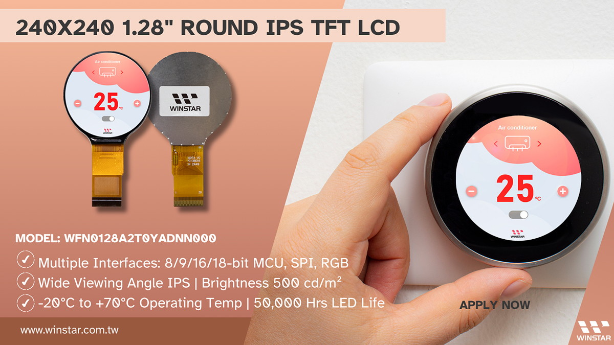
GC9A01 1.28인치 TFT 원형 LCD 모듈 (모델: WFN0128A2T0YADNN000)은 240x240 IPS 고해상도 디스플레이를 제공하여 원형 디스플레이가 필요한 애플리케이션에 이상적인 솔루션입니다. 까다로운 환경을 위해 설계된 이 컴팩트한 모듈은 뛰어난 성능과 내구성을 자랑하며, 다양한 시스템에 쉽게 통합할 수 있습니다.
GC9A01 드라이버 IC를 탑재한 이 모듈은 8/9/16/18비트 MCU, 3/4선 SPI 직렬, 16/18비트 RGB 등 유연한 인터페이스 옵션을 지원하여 다양한 호스트 플랫폼과 호환성을 제공합니다. 500 cd/m²의 밝기와 700:1의 높은 명암비로 다양한 조도 환경에서도 안정적인 성능을 발휘합니다. 또한 -20℃에서 +70℃까지의 넓은 동작 온도 범위를 갖추고 있으며, 50,000시간의 긴 LED 수명을 자랑하여 장기적으로 신뢰할 수 있고 비용 효율적인 솔루션을 제공합니다.
GC9A01 1.28인치 TFT 원형 LCD 디스플레이는 컴팩트하고 고성능의 원형 디스플레이가 필요한 애플리케이션에 이상적인 선택입니다. 유연한 인터페이스 옵션, 넓은 온도 범위 및 긴 사용 수명을 제공하며, 산업 및 소비자급 장치 모두의 요구를 충족하도록 설계되었습니다.
| 항목 | 치수 | 단위 |
|---|---|---|
| 크기 (대각선) | 1.28 | 인치 |
| 도트 매트릭스 | 240 × RGB × 240 (TFT) | 점 |
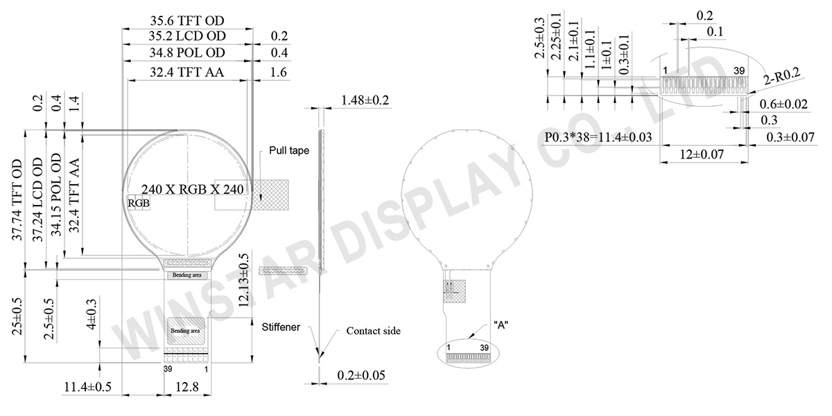
| 모듈 치수 | 35.6 × 37.74 × 1.48 | mm |
| 활성 영역 | 32.4 × 32.4 | mm |
| 도트 피치 | 0.135 × 0.135 | mm |
| LCD 유형 | TFT, 검은색, 투과성 | |
| 시야각 | 85/85/85/85 | |
| TFT 인터페이스 | 8/9/16/18bit MCU 3/4SPI+16/18BIT RGB 3/4 Serial |
|
| 역광 타입 | LED ,백색 | |
| 드라이버 IC | GC9A01 | |
| 터치 패널 | 터치패널(스크린)이 없는 | |
| 표면 | 눈부심 방지 | |
| 항목 | 기호 | 최소값 | 대표값 | 최대값 | 단위 |
|---|---|---|---|---|---|
| 작동 온도 | TOP | -20 | - | +70 | ℃ |
| 보관 온도 | TST | -30 | - | +80 | ℃ |
| 항목 | 기호 | 최소값 | 대표값 | 최대값 | 단위 |
|---|---|---|---|---|---|
| Digital Supply Voltage | VCC | 2.5 | 2.8 | 3.3 | V |
| Digital interface supple Voltage | IOVCC | 1.65 | 2.8 | 3.3 | V |
| Normal mode Current consumption | ICC | -- | 6 | 12 | mA |
| Level input voltage | VIH | 0.7*IOVCC | -- | IOVCC | V |
| VIL | GND | -- | 0.3*IOVCC | V | |
| Level output voltage | VOH | 0.8*IOVCC | -- | IOVCC | V |
| VOL | GND | -- | 0.2*IOVCC | V |
| 항목 | 기호 | 최소값 | 대표값 | 최대값 | 단위 |
|---|---|---|---|---|---|
| LED 전류 | - | - | 40 | - | mA |
| LED 전압 | VLED+ | 2.8 | 3.0 | 3.2 | V |
| LED 수명 | - | 50000 | - | - | Hr |
| Pin No | 기호 | 기능 | I/O |
|---|---|---|---|
| 1 | VLED+ | Anode pin of backlight | P |
| 2 | VLED* | Cathode pin of backlight | P |
| 3 | GND | Ground. | P |
| 4 | GND | Ground. | P |
| 5 | VCC | Supply voltage (2.5-3.3V). | P |
| 6 | IOVCC | Supply voltage (1.65-3.3V). | P |
| 7 | RESET | This signal will reset the device and must be applied to properly initialize the chip. |
I |
| 8 | WR(SPI-RS) | -Write enable in MCU parallel interface. Display data/command selection pin in 4-line serial interface. Second Data lane in 2 data lane serial interface. -If not used, please fix this pin at IOVCC or GND. |
I |
| 9 | CS | Chip select input pin (“Low” enable ,CSX). Fix this pin at IOVCC or GND when not in use. |
I |
| 10 | RS(SPI-SCL) | -Display data/command selection pin in parallel interface.(D/CX) -This pin is used to be serial interface clock. (SCL) DC=’1’: display data or parameter. DC=’0’: command data. -If not used, please fix this pin at IOVCC or GND. |
I |
| 11 | RD | Serves as a read signal and MCU read data at the rising edge. Fix this pin at IOVCC or GND when not in use. |
I |
| 12 | PCLK | Dot clock signal for RGB interface operation. (DOTCLK) Fix this pin at IOVCC or GND when not in use. |
I |
| 13 | DE | Data enable signal for RGB interface operation. (ENABLE) fix this pin at IOVCC or GND when not in use. |
I |
| 14 | VSYNC | Frame synchronizing signal for RGB interface operation. fix this pin at IOVCC or GND when not in use. |
I |
| 15 | HSYNC | Line synchronizing signal for RGB interface operation. fix this pin at IOVCC or GND when not in use. |
I |
| 16 | TE | Tearing effect output pin to synchronize MPU to frame writing, activated by S/W command. When this pin is not activated, this pin is low. If not used, open this pin. |
I |
| 17 | NC | No connection | O |
| 18 | SDA | The data is latched on the rising edge of the SCL signal. If not used, please fix this pin at IOVCC or GND level |
I/O |
| 19-36 | DB17-DB0 | 18-bit parallel bi-directional data bus for MCU system and RGB interface mode . 18-bit RGB DB0:BLUE LSB--DB5:BLUE MSB; DB6:GREEN LSB--DB11:GREEN,MSB; DB12:RED LSB--DB17:RED MSB. 16-bit RGB: DB1:BLUE LSB--DB5:BLUE MSB; DB6:GREEN LSB--DB11:GREEN,MSB; DB13:RED LSB--DB17:RED MSB. mode Fix to GND level when not in use |
I/O |
| 37 | IM0 | MPU Parallel interface bus and serial interface select If use RGB Interface must select serial interface. Fix this pin at IOVCC and GND. |
I |
| 38 | IM1 | ||
| 39 | IM3 |
| IM3 | IM1 | IM0 | Interface Type | DB Pin in use |
|---|---|---|---|---|
| L | L | L | 8080 MCU 8-bit bus interface | DB7-DB0 |
| L | H | L | 8080 MCU 16-bit bus interface | DB15- DB0 |
| L | L | H | 8080 MCU 9-bit bus interface | DB8- DB0 |
| L | H | H | 8080 MCU 18-bit bus interface | DB17- DB0 |
| H | L | H | 3-wire 9-bit data serial interface | SDA:In/Out |
| 2 data line serial interface | SDA:In/Out,DCX:In | |||
| H | H | H | 4-wire 8-bit data serial interface | SDA:In/Out |

"모든 쿠키 허용"을 클릭하면 사이트 탐색을 개선하고, 사이트 사용을 분석하며, 마케팅 및 성능 노력에 도움을 주기 위해 쿠키를 귀하의 장치에 저장하는 데 동의한 것으로 간주됩니다. 이 주제에 대한 추가 정보는 당사의 정책에서 확인할 수 있습니다. 개인정보 보호정책