 - WEO012832N")
我們重視您的隱私
通過點擊「允許所有 Cookie」,代表您同意在您的設備上存儲 Cookie 以增強網站瀏覽體驗、分析網站使用情況並協助我們的行銷和網站效能優化工作。您可以在我們的隱私權政策中找到有關於此的更多資訊。

 搭配 PCB - WEP012832N")
 搭配 PCB - WEP012832N")
 搭配 PCB - WEP012832N")
 搭配 PCB - WEP012832N")
 搭配 PCB - WEP012832N")
 搭配 PCB - WEP012832N")
 搭配 PCB - WEP012832N")
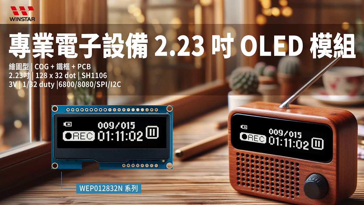
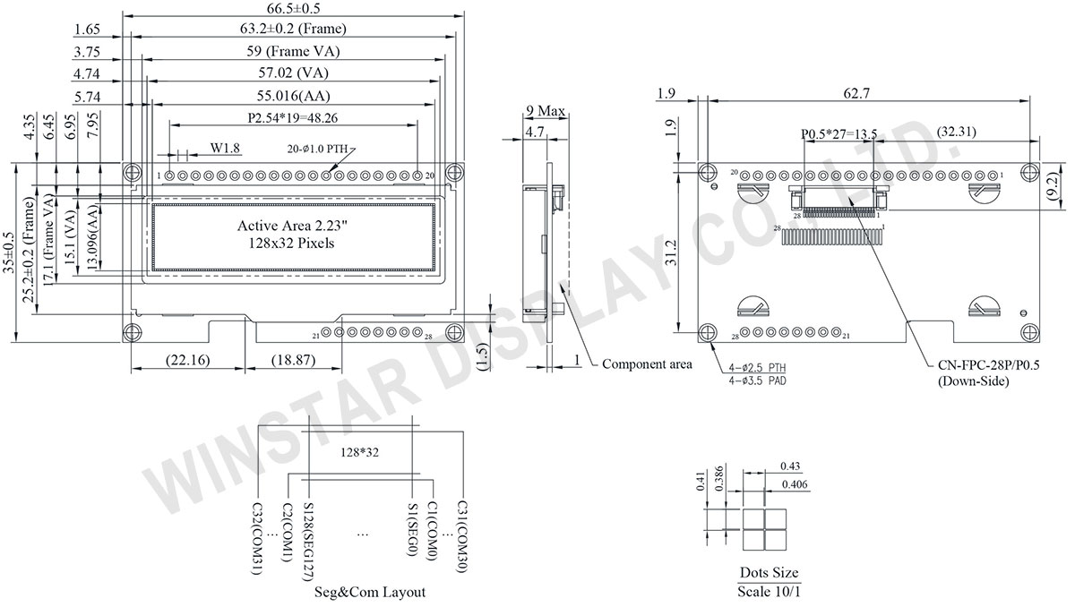
WEP012832N是一款設計有PCB板的COG繪圖型OLED模組,解析度為128x32 dots,對角線尺寸為2.23吋(有效區域:55.016 × 13.096 mm)。模組包括內建 SH1106 驅動IC,支援透過 6800、8080 並列介面、4 線 SPI 、I2C 串列介面進行通訊。邏輯電源電壓範圍為2.9V~3.5V,典型值為3.3V。以 1/32 duty驅動方式運行,提供內部升壓及外部供電功能。此系列配備金屬鐵框和螺絲孔,方便模組安裝,對比度(典型值)為10,000:1。
WEP012832N 系列移除固定pin針,可依客戶需求半客製不同長度Pin針。 PCB設計保留了整合式電容式觸控面板的空間,無需重新開發,確保靈活性,滿足不同客戶的需求。
WEP012832N 非常適合錄音筆、血糖儀、MP3 播放器、迷你音響、迷你收音機和醫療儀器等應用,工作溫度範圍為 -40℃~+80℃,儲存溫度範圍為 -40℃~+85℃。
Data source ref:WEP012832NWPP3N00000
| 項目 | 規格 | 單位 |
|---|---|---|
| 解析度 | 128 × 32 Dots | - |
| 模組尺寸 | 66.5 × 35.0 × 9 | mm |
| 有效區域 | 55.016 × 13.096 | mm |
| 像素大小 | 0.406 × 0.386 | mm |
| 像素間距 | 0.43 × 0.41 | mm |
| 顯示模式 | 被動矩陣 | |
| 顯示顏色 | 單色 | |
| 驅動方式 | 1/32 Duty | |
| IC | SH1106 | |
| 介面 | 6800,8080,4線SPI,I2C | |
| 尺寸 | 2.23 吋 | |
| 參數 | 符號 | 最小值 | 最大值 | 單位 |
|---|---|---|---|---|
| 邏輯電源電壓 | VDD-VSS | -0.3 | 3.6 | V |
| 工作溫度 | TOP | -40 | +80 | °C |
| 儲存溫度 | TSTG | -40 | +85 | °C |
| 項目 | 符號 | 條件 | 最小值 | 典型值 | 最大值 | 單位 |
|---|---|---|---|---|---|---|
| 邏輯電源電壓 | VDD | - | 2.9 | 3.3 | 3.5 | V |
| 輸入高電壓 | VIH | - | 0.8XVDD | - | VDD | V |
| 輸入低電壓 | VIL | - | VSS | - | 0.2xVDD | V |
| 輸出高電壓 | VOH | - | 0.8xVDD | - | VDD | V |
| 輸出低電壓 | VOL | - | VSS | - | 0.2xVDD | V |
| Display 50% Pixel On | IDD | VDD=3.3V | - | 75 | 110 | mA |
| No. | 符號 | 功能 | |||||||||||||||
|---|---|---|---|---|---|---|---|---|---|---|---|---|---|---|---|---|---|
| 1 | VSS | Ground. | |||||||||||||||
| 2 | VDD | Power supply input. | |||||||||||||||
| 3 | NC | No connection. | |||||||||||||||
| 4 | D/C# | This is the Data/Command control pad that determines whether the data bits are data or a command. D/C = “H”: the inputs at DB0 to DB7 are treated as display data. D/C = “L”: the inputs at DB0 to DB7 are transferred to the command registers. In I2C interface, this pad serves as SA0 to distinguish the different address of OLED driver. |
|||||||||||||||
| 5 | R/W# | This is a MPU interface input pad. When connected to an 8080 MPU, this is active LOW. This pad connects to the 8080 MPU WR signal. The signals on the data bus are latched at the rising edge of the WR signal. When connected to a 6800 Series MPU: This is the read/write control signal input terminal. When R/W = “H”: Read. When R/W = “L”: Write. |
|||||||||||||||
| 6 | E/RD# | This is a MPU interface input pad. When connected to an 8080 series MPU, it is active LOW. This pad is connected to the RD signal of the 8080 series MPU, and the data bus is in an output status when this signal is “L”. When connected to a 6800 series MPU, this is active HIGH. This is used as an enable clock input of the 6800 series MPU. When RD = “H”: Enable. When RD = “L”: Disable. |
|||||||||||||||
| 7~14 | DB0~DB7 | This is an 8-bit bi-directional data bus that connects to an 8-bit or 16-bit standard MPU data bus. When the serial interface is selected, then D0 serves as the serial clock input pad (SCL) and D1 serves as the serial data input pad (SI). At this time, D2 to D7 are set to high impedance. When the I2C interface is selected, then D0 serves as the serial clock input pad (SCL) and D1 serves as the serial data input pad (SDAI). At this time, D2 to D7 are set to high impedance. |
|||||||||||||||
| 15 | CS# | This pad is the chip select input. When CS = “L”, then the chip select becomes active, and data/command I/O is enabled. | |||||||||||||||
| 16 | RES# | This is a reset signal input pad. When RES is set to “L”, the settings are initialized. The reset operation is performed by the RES signal level. | |||||||||||||||
| 17 | BS1 | These are the MPU interface mode select pads.
|
|||||||||||||||
| 18 | BS2 | ||||||||||||||||
| 19 | NC | No connection. | |||||||||||||||
| 20 | FG | Ground. | |||||||||||||||
| 21~25 | NC | No connection. | |||||||||||||||
| 26 | VSS | Ground. | |||||||||||||||
| 27~28 | NC | No connection. |

通過點擊「允許所有 Cookie」,代表您同意在您的設備上存儲 Cookie 以增強網站瀏覽體驗、分析網站使用情況並協助我們的行銷和網站效能優化工作。您可以在我們的隱私權政策中找到有關於此的更多資訊。