我們重視您的隱私
通過點擊「允許所有 Cookie」,代表您同意在您的設備上存儲 Cookie 以增強網站瀏覽體驗、分析網站使用情況並協助我們的行銷和網站效能優化工作。您可以在我們的隱私權政策中找到有關於此的更多資訊。


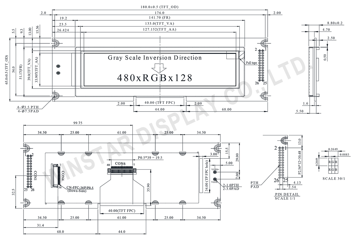
WF52QTLBSDBN0 型號是單色繪圖型STN的WG24064A COB模組升級為彩色TFT模組而是設計的產品,同樣是 5.2吋的模組但是 WF52QTLBSDBN0 的解析度是 480x128 像素 為 WG24064A 的2倍解析度。WF52QTLBSDBN0 含 SSD1963 IC的控制板,外觀尺寸規格與單色STN WG24064A相同,客戶可以直接替代升級為彩色TFT模組。
WF52QTLBSDBN0 的模組的尺寸為 180.0 x 65.0 mm 與 WG24064A 完全相同。而且產品設計也考量Pin-to-Pin的介面,此款型號模組含 SSD1963 的控制板,支援8080 MPU 8bit /16 bit 並列介面,WF52QTLBSDBN0 設計兩種介面供客戶選擇: 一種是 26 pins 8 bits 使用 pin header 排針或是一般 TFT 最常使用的 8080 MPU 8 bits/16 bits ZIF connector 介面 (36 pins)。
此款模組設計兩種介面,所以有兩組Pin Define,分別為CON1 與CON4。CON1是提供給原來使用STN繪圖型WG24064A升級為彩色TFT的客戶所設計的,可使用 26 pins 的 pin header 排針。WG24064A是使用20 pins的傳統PCB through hole, 以A.K腳點亮背光,而WF52QTLBSDBN0前20 pins則是與WG24064A為pin-to-pin,使用pin 21與pin 22點背光,如需要詳細的產品規格書或是相關CON1 與CON4的腳位定義資料,請與我們的業務人員聯繫。
| 項目 | 規格 | 單位 |
|---|---|---|
| 對角線尺寸 | 5.2 | 吋 |
| 解析度 | 480 x RGBx128 | dots |
| 模組尺寸 | 180.0 x 65.0 x 8.8 | mm |
| 有效區域 | 127.152 x 33.9072 | mm |
| 點間距 | 0.0883 x 0.2649 | mm |
| LCD類型 | TFT, 正常白, 透射性 | |
| 視角 | 6點鐘方向 | |
| 灰階反轉 | 12點鐘方向 | |
| 長寬比 | Bar Type | |
| 背光類型 | LED, 正常白 | |
| 控制器IC | SSD1963 | |
| 介面 | Digital 8080 family MPU 8bit/16bit | |
| 觸控面板類型 | 無觸控面板 | |
| 表面 | 亮面 | |
| 項目 | 符號 | 最小值 | 典型值 | 最大值 | 單位 |
|---|---|---|---|---|---|
| 工作溫度 | TOP | -20 | - | +70 | ℃ |
| 儲存溫度 | TST | -30 | - | +80 | ℃ |
| 項目 | 符號 | 條件 | 最小值 | 典型值 | 最大值 | 單位 |
|---|---|---|---|---|---|---|
| LCM供電電壓 | VDD | - | 3.0 | 3.1 | 3.3 | V |
| LCM供電電流 | IDD | - | - | 200 | - | mA |
| Pin | 符號 | 功能說明 |
|---|---|---|
| 1 | GND | System round pin of the IC. Connect to system ground. |
| 2 | VDD | Power Supply : +3.3V |
| 3 | BL_E | Backlight control signal , H: On \ L: Off |
| 4 | D/C | Data/Command select |
| 5 | WR | Write strobe signal |
| 6 | RD | Read strobe signal |
| 7 | DB0 | Data bus |
| 8 | DB1 | Data bus |
| 9 | DB2 | Data bus |
| 10 | DB3 | Data bus |
| 11 | DB4 | Data bus |
| 12 | DB5 | Data bus |
| 13 | DB6 | Data bus |
| 14 | DB7 | Data bus |
| 15 | DB8 | Data bus (When select 8bits mode, this pin is NC) |
| 16 | DB9 | Data bus (When select 8bits mode, this pin is NC) |
| 17 | DB10 | Data bus (When select 8bits mode, this pin is NC) |
| 18 | DB11 | Data bus (When select 8bits mode, this pin is NC) |
| 19 | DB12 | Data bus (When select 8bits mode, this pin is NC) |
| 20 | DB13 | Data bus (When select 8bits mode, this pin is NC) |
| 21 | DB14 | Data bus (When select 8bits mode, this pin is NC) |
| 22 | DB15 | Data bus (When select 8bits mode, this pin is NC) |
| 23 | NC | No connect |
| 24 | NC | No connect |
| 25 | CS | Chip select |
| 26 | RESET | Hardware reset |
| 27 | LR | Right /Left selection; Default R/L is Pull High |
| 28 | UD | Up/down selection; Default U/D is Pull High |
| 29 | NC | No connection |
| 30 | NC | No connection |
| 31 | NC | No connection |
| 32 | NC | No connection |
| 33 | VLED- | VLED- for B/L LED inverter (GND) |
| 34 | VLED- | VLED- for B/L LED inverter (GND) |
| 35 | VLED+ | VLED+ for B/L LED inverter (+5V) |
| 36 | VLED+ | VLED+ for B/L LED inverter (+5V) |
| Pin | 符號 | 功能說明 |
|---|---|---|
| 1 | NC(FG) | No connect (Frame Grand) |
| 2 | GND | System round pin of the IC. Connect to system ground. |
| 3 | VDD | Power Supply : +3.3V |
| 4 | BLE | Backlight control signal , H: On \ L: Off |
| 5 | WR | Write strobe signal |
| 6 | RD | Read strobe signal |
| 7 | CS | Chip select |
| 8 | D/C | Data/Command select |
| 9 | NC | No connect |
| 10 | RESET | Hardware reset |
| 11 | DB0 | Data bus |
| 12 | DB1 | Data bus |
| 13 | DB2 | Data bus |
| 14 | DB3 | Data bus |
| 15 | DB4 | Data bus |
| 16 | DB5 | Data bus |
| 17 | DB6 | Data bus |
| 18 | DB7 | Data bus |
| 19 | NC | No connect |
| 20 | NC | No connect |
| 21 | VLED+ | VLED+ for B/L LED inverter (+5V) |
| 22 | VLED- | VLED- for B/L LED inverter (GND) |
| 23 | NC | No connect |
| 24 | NC | No connect |
| 25 | NC | No connect |
| 26 | GND | System round pin of the IC. Connect to system ground. |

通過點擊「允許所有 Cookie」,代表您同意在您的設備上存儲 Cookie 以增強網站瀏覽體驗、分析網站使用情況並協助我們的行銷和網站效能優化工作。您可以在我們的隱私權政策中找到有關於此的更多資訊。