 - WEA012864AA")
私たちはあなたのプライバシーを大切にします
「すべてのクッキーを許可」をクリックすると、サイトのナビゲーションを向上させ、サイト使用状況を分析し、マーケティングおよびパフォーマンスの取り組みを支援するために、クッキーをデバイスに保存することに同意したことになります。この件に関する詳細情報は、ポリシーをご覧ください。プライバシーポリシー


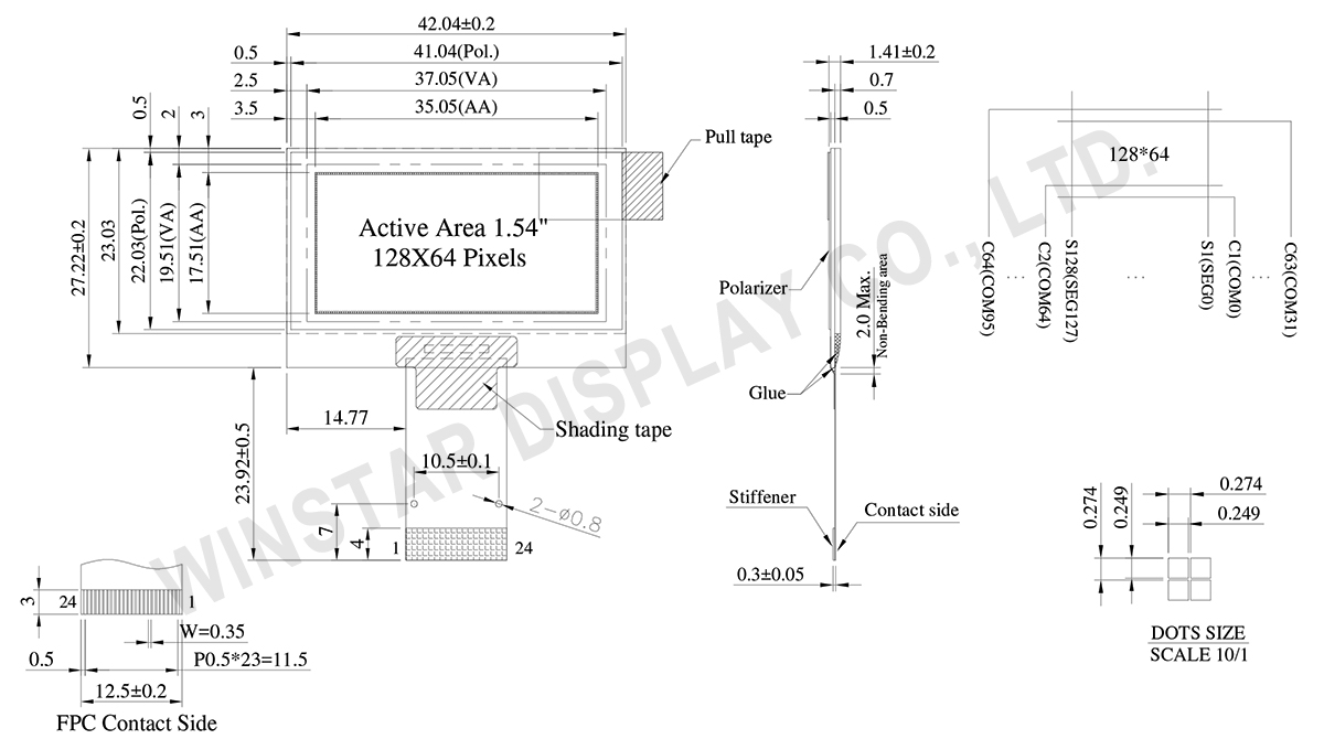
WEO012864AA は、1.54インチ 128×64 解像度の COG 有機ELディスプレイモジュールで、SSD1327 ドライバ IC を搭載しています。 6800/8080 パラレル、4 線式 SPI、I2C インターフェースに対応し、16 階調(4 ビット)グレースケール表示が可能です。 ロジック電源電圧は 3V です。 50% チェッカーボード表示時の代表的な表示電流は、12.5V VCC において、白色有機ELが 10 mA、黄色有機ELが 7 mA、駆動デューティは 1/64 です。 グレースケール表示が不要な用途には、WEO012864A モデルも用意されています。
チップ・オン・ガラス(COG)技術を採用し、モジュール厚はわずか 1.41 mm の薄型設計です。 低消費電力かつ軽量な特長を備えており、壁掛けメーター、家電機器、POS システム、クラウド/IoT アプリケーション、携帯型計測機器、各種インテリジェント機器、エネルギー関連機器、通信機器、医療機器など、幅広い用途に適しています。 動作温度範囲は -40°C ~ +80°C、保存温度範囲は -40°C ~ +85°C です。
| 項目 | 仕様 | 単位 |
|---|---|---|
| ドットマトリックス(解像度) | 128 x 64 | - |
| モジュールサイズ | 42.04 × 27.22 × 1.41 | mm |
| 有効エリア | 35.05 × 17.51 | mm |
| ドットサイズ | 0.249 × 0.249 | mm |
| ドットピッチ | 0.274 × 0.274 | mm |
| 表示モード | パッシブマトリックス | |
| 発光色 | モノクロ | |
| 駆動方法 | 1/64 Duty | |
| IC | SSD1327 | |
| インターフェイス | 6800/8080/4-Wire SPI/I2C | |
| 表示サイズ(対角線) | 1.54 インチ | |
| パラメーター | 記号 | 最小値 | 最大値 | 単位 |
|---|---|---|---|---|
| 低電圧電源, 入力/出力ピンの電源電圧 | VCI | -0.3 | 4.0 | V |
| ロジック電源電圧 | VDD | -0.5 | 2.75 | V |
| Display電源電圧 | VCC | -0.5 | 19.0 | V |
| 操作温度 | TOP | -40 | +80 | °C |
| 保存温度 | TSTG | -40 | +85 | °C |
| 項目 | 記号 | 条件 | 最小値 | 典型値 | 最大値 | 単位 |
|---|---|---|---|---|---|---|
| 低電圧電源, 入力/出力ピンの電源電圧 | VCI | - | 1.65 | 3.0 | 3.5 | V |
| Display電源電圧 | VCC | - | 8.0 | 12.5 | 13.0 | V |
| ロジック電源電圧 | VDD | - | 1.65 | - | 2.6 | V |
| 高レベル入力 | VIH | - | 0.8×VCI | - | VCI | V |
| 低レベル入力 | VIL | - | 0 | - | 0.2×VCI | V |
| 高レベル出力 | VOH | - | 0.9×VCI | - | VCI | V |
| 低レベル出力 | VOL | - | 0 | - | 0.1×VCI | V |
| 50% Check Board operating Current | ICC | VCC =12.5V | - | 10 | 20 | mA |
| Pin No. | 記号 | 説明 | |||||||||||||||
|---|---|---|---|---|---|---|---|---|---|---|---|---|---|---|---|---|---|
| 1 | VSS | This is a ground pin. | |||||||||||||||
| 2 | VCC | Power supply for panel driving voltage. | |||||||||||||||
| 3 | VCOMH | COM signal deselected voltage level. A capacitor should be connected between this pin and VSS. No external power supply is allowed to connect to this pin. |
|||||||||||||||
| 4 | VCI | Low voltage power supply and power supply for interface logic level. It should match with the MCU interface voltage level and must be connected to external source. VCI must always set to be equivalent to or higher than VDD. |
|||||||||||||||
| 5 | VDD | Power supply pin for core logic operation. VDD can be supplied externally (within the range of 2.4V to 2.6V) or regulated internally from VCI. A capacitor should be connected between VDD and VSS under all circumstances. |
|||||||||||||||
| 6 | BS1 | Communicating Protocol Select These pins are MCU interface selection input. See the following table:
|
|||||||||||||||
| 7 | BS2 | ||||||||||||||||
| 8 | VSS | This is a ground pin. | |||||||||||||||
| 9 | IREF | This pin is the segment output current reference pin. A resistor should be connected between this pin and VSS to maintain the current around 10uA. |
|||||||||||||||
| 10 | CS# | This pin is the chip select input. The chip is enabled for MCU communication only when CS# is pulled low. | |||||||||||||||
| 11 | RES# | This pin is reset signal input. When the pin is low, initialization of the chip is executed. | |||||||||||||||
| 12 | D/C# | This pin is Data/Command control pin connecting to the MCU. When the pin is pulled HIGH, the data at D[7:0] will be interpreted as data. When the pin is pulled LOW, the data at D[7:0] will be transferred to a command register. In I2C mode, this pin acts as SA0 for slave address selection. |
|||||||||||||||
| 13 | R/W# (WR#) | This pin is read / write control input pin connecting to the MCU interface. When 6800 interface mode is selected, this pin will be used as Read/Write (R/W#) selection input. Read mode will be carried out when this pin is pulled HIGH and write mode when LOW. When 8080 interface mode is selected, this pin will be the Write (WR#) input. Data write operation is initiated when this pin is pulled LOW and the chip is selected. When serial or I2C interface is selected, this pin must be connected to VSS. |
|||||||||||||||
| 14 | E/RD# | This pin is MCU interface input. When 6800 interface mode is selected, this pin will be used as the Enable (E) signal. Read/write operation is initiated when this pin is pulled HIGH and the chip is selected. When 8080 interface mode is selected, this pin receives the Read (RD#) signal. Read operation is initiated when this pin is pulled LOW and the chip is selected. When serial or I2C interface is selected, this pin must be connected to VSS. |
|||||||||||||||
| 15 | D0 | These pins are 8-bit bi-directional data bus to be connected to the microprocessor’s data bus. When serial mode is selected, D1 will be the serial data input SDIN and D0 will be the serial clock input SCLK. | |||||||||||||||
| 16 | D1 | ||||||||||||||||
| 17 | D2 | ||||||||||||||||
| 18 | D3 | ||||||||||||||||
| 19 | D4 | ||||||||||||||||
| 20 | D5 | ||||||||||||||||
| 21 | D6 | ||||||||||||||||
| 22 | D7 | ||||||||||||||||
| 23 | VCC | Power supply for panel driving voltage. | |||||||||||||||
| 24 | VSS | This is a ground pin. |

「すべてのクッキーを許可」をクリックすると、サイトのナビゲーションを向上させ、サイト使用状況を分析し、マーケティングおよびパフォーマンスの取り組みを支援するために、クッキーをデバイスに保存することに同意したことになります。この件に関する詳細情報は、ポリシーをご覧ください。プライバシーポリシー