
我們重視您的隱私
通過點擊「允許所有 Cookie」,代表您同意在您的設備上存儲 Cookie 以增強網站瀏覽體驗、分析網站使用情況並協助我們的行銷和網站效能優化工作。您可以在我們的隱私權政策中找到有關於此的更多資訊。


| Pin No. | 符號 | Level | 說明 | |||||||||||||||||||||||||||||||||||||||||||||
|---|---|---|---|---|---|---|---|---|---|---|---|---|---|---|---|---|---|---|---|---|---|---|---|---|---|---|---|---|---|---|---|---|---|---|---|---|---|---|---|---|---|---|---|---|---|---|---|---|
| 1 | VB1- | PWR | LCD Bias Voltages. These are the voltage source to provide SEG driving currents. These voltages are generated internally. Connect capacitors of CBX between VBX+ and VBX–. The resistance of these four traces directly affects the SEG driving strength of the resulting LCD module. Minimize the trace resistance is critical in achieving high quality image. |
|||||||||||||||||||||||||||||||||||||||||||||
| 2 | VB1+ | |||||||||||||||||||||||||||||||||||||||||||||||
| 3 | VB0- | |||||||||||||||||||||||||||||||||||||||||||||||
| 4 | VB0+ | |||||||||||||||||||||||||||||||||||||||||||||||
| 5 | VLCD | PWR | Main LCD Power Supply. Connect these pins together. | |||||||||||||||||||||||||||||||||||||||||||||
| 6 | VBIAS | I | This is the reference voltage to generate the actual SEG driving voltage. VBIAS can be used to fine tune VLCD by external variable resistors. Internal resistor network has been provided to simplify external trimming circuit. In COF application, connect a small bypass capacitor between VBIAS and VSS to reduce noise. |
|||||||||||||||||||||||||||||||||||||||||||||
| 7 | VSS | PWR | Ground | |||||||||||||||||||||||||||||||||||||||||||||
| 8 | VDD | PWR | Supply Voltage for logic | |||||||||||||||||||||||||||||||||||||||||||||
| 9 | D7 | I/O | Bi-directional bus for both serial and parallel host interfaces. In serial modes, connect D[0] to SCK, D[3] to SDA,
|
|||||||||||||||||||||||||||||||||||||||||||||
| 10 | D6 | |||||||||||||||||||||||||||||||||||||||||||||||
| 11 | D5 | |||||||||||||||||||||||||||||||||||||||||||||||
| 12 | D4 | |||||||||||||||||||||||||||||||||||||||||||||||
| 13 | D3 | |||||||||||||||||||||||||||||||||||||||||||||||
| 14 | D2 | |||||||||||||||||||||||||||||||||||||||||||||||
| 15 | D1 | |||||||||||||||||||||||||||||||||||||||||||||||
| 16 | D0 | |||||||||||||||||||||||||||||||||||||||||||||||
| 17 | WR1 | I | WR[1:0] controls the read/write operation of the host interface. See Host Interface section for more detail. In parallel mode, WR[1:0] meaning depends on whether the interface is in the 6800 mode or the 8080 mode. In serial interface modes, these two pins are not used, connect them to VSS. |
|||||||||||||||||||||||||||||||||||||||||||||
| 18 | WR0 | |||||||||||||||||||||||||||||||||||||||||||||||
| 19 | CD | I | Select Control data or Display data for read/write operation. In S9 mode, CD pin is not used. Connect CD to VSS when not used. ”L”: Control data ”H”: Display data | |||||||||||||||||||||||||||||||||||||||||||||
| 20 | RST | I | When RST=”L”, all control registers are re-initialized by their default states. Since UC1608x has built-in Power-ON-Reset and Software Reset command, RST pin is not required for proper chip operation. When RST is not used, connect the pin to VDD. |
|||||||||||||||||||||||||||||||||||||||||||||
| 21 | CS | I | Chip Select. The chip is selected when CS=”H”. When the chip is not selected, D[7:0] will be high impedance. | |||||||||||||||||||||||||||||||||||||||||||||
| 22 | BM0 | I | Bus mode: The interface bus mode is determined by BM[1:0] and D[7:6] by the following relationship:
|
|||||||||||||||||||||||||||||||||||||||||||||
| 23 | BM1 |
| 項目 | 標準尺寸 | 單位 |
|---|---|---|
| 顯示形式 | 240 x 128 點 | - |
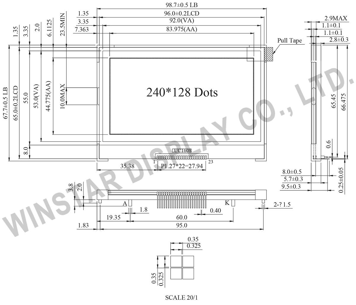
| 模組尺寸 | 98.7 x 67.7 x 9.5 (Max) | mm |
| 檢視區域 | 92.0 x 53.0 | mm |
| 有效區域 | 83.975 x 44.775 | mm |
| 點大小 | 0.325 x0.325 | mm |
| 點間距 | 0.35 x 0.35 | mm |
| 驅動方式 | 1/128 , 1/12 Bias | |
| 背光類型 | LED | |
| IC | UC1608 | |
| 介面 | 6800/8080/3 wire SPI/4 wire SPI | |
| 項目 | 符號 | 最小值 | 典型值 | 最大值 | 單位 |
|---|---|---|---|---|---|
| 工作溫度 | TOP | -20 | - | +70 | ℃ |
| 儲存溫度 | TST | -30 | - | +80 | ℃ |
| 邏輯電源電壓 | VDD | -0.3 | - | +4.0 | V |
| LCD Generator supply voltage | VDD2 | -0.3 | - | +4.0 | V |
| LCD Generated voltage | VLCD | -0.3 | - | +17.8 | V |
| 項目 | 符號 | 條件 | 最小值 | 典型值 | 最大值 | 單位 |
|---|---|---|---|---|---|---|
| 邏輯電源電壓 | VDD-VSS | - | 2.7 | 2.8~3.3 | 3.6 | V |
| LCM電源電壓 | V0-VSS | Ta=-20℃ Ta=25℃ Ta=70℃ |
- 15.2 - |
- 15.5 - |
- 15.8 - |
V V V |
| 輸入高電壓 | VIH | - | 0.8 VDD | - | - | V |
| 輸入低電壓 | VIL | - | - | - | 0.2VDD | V |
| 輸出高電壓 | VOH | - | 0.8VDD | - | - | V |
| 輸出低電壓 | VOL | - | - | - | 0.2VDD | V |
| 電源電流(不包括LED背光) | IDD | VDD=3.0V | - | 1.1 | - | mA |

通過點擊「允許所有 Cookie」,代表您同意在您的設備上存儲 Cookie 以增強網站瀏覽體驗、分析網站使用情況並協助我們的行銷和網站效能優化工作。您可以在我們的隱私權政策中找到有關於此的更多資訊。