


우리는 귀하의 프라이버시를 소중히 여깁니다
"모든 쿠키 허용"을 클릭하면 사이트 탐색을 개선하고, 사이트 사용을 분석하며, 마케팅 및 성능 노력에 도움을 주기 위해 쿠키를 귀하의 장치에 저장하는 데 동의한 것으로 간주됩니다. 이 주제에 대한 추가 정보는 당사의 정책에서 확인할 수 있습니다. 개인정보 보호정책


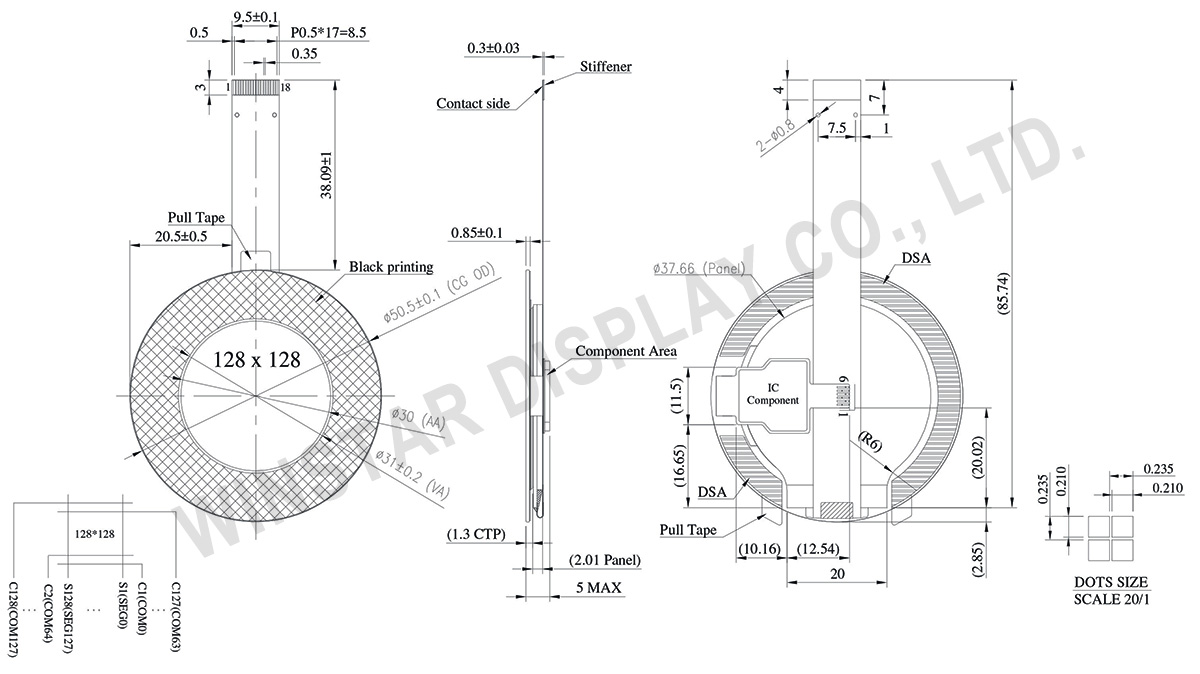
WEO128128D-CTP는 지름 1.18인치의 원형 OLED 디스플레이로, 모듈에는 용량식 터치 스크린이 통합되어 있으며, 해상도는 128x128 도트입니다. 이 모듈은 SSD1327 IC가 장착되어 있어 4선식 SPI 및 I2C 인터페이스를 지원하며, 전압 공급은 3V(일반값)이며 1/128 구동 듀티를 갖추고 있습니다. 또한, WEO128128D-CTP 모델에는 모듈에 통합된 FT3268 터치 패널 IC가 있어 I2C 인터페이스를 지원하고 용량식 터치 스크린을 위한 단일 감지 지점을 제공합니다.
이 원형 OLED WEO128128D CTP 모델은 스마트 홈 응용, 지능형 기술 기기, 에너지 시스템, 통신 시스템, 의료 기기 등에 적합합니다. 10,000:1의 높은 명암비와 최대 160°까지 확장 가능한 시야각을 자랑하며, 이 OLED 모듈은 더욱 선명한 디스플레이 이미지를 보장합니다. 이 모듈은 -20℃에서 +70℃의 온도 범위 내에서 작동하도록 설계되어 있으며, 저장 온도는 -30℃에서 +70℃로 범위합니다.
| 항목 | 치수 | 단위 |
|---|---|---|
| 도트 매트릭스 | 128 × 128 | Dots |
| 모듈 치수 | Ø50.5 × 5.0 | mm |
| 활성 영역 | Ø30.0 | mm |
| 도트 크기 | 0.210 × 0.210 | mm |
| 도트 피치 | 0.235 × 0.235 | mm |
| 디스플레이 모드 | 패시브 매트릭스 (Passive Matrix) | |
| 디스플레이 색 | Monochrome | |
| Drive Duty | 1/128 Duty | |
| 그레이스케일 | 4 bits | |
| IC | SSD1327 | |
| 인터페이스 | 4-line SPI , I2C | |
| 크기 (대각선) | 1.18 인치 | |
| CTP IC | FT3268 |
| 터치포인트 | 1 |
| CTP 인터페이스 | I2C |
| Parameter | 기호 | 최소값 | 최대값 | 단위 |
|---|---|---|---|---|
| Supply Voltage for Operation | VCI | -0.3 | 4.0 | V |
| Supply Voltage for Logic | VDD | -0.5 | 2.75 | V |
| Supply Voltage for Display | VCC | -0.5 | 19.0 | V |
| 작동 온도 | TOP | -20 | +70 | °C |
| 보관 온도 | TSTG | -30 | +70 | °C |
| 항목 | 기호 | 조건 | 최소값 | 대표값 | 최대값 | 단위 |
|---|---|---|---|---|---|---|
| Supply Voltage for Operation | VCI | - | 2.8 | 3.0 | 3.3 | V |
| Supply Voltage for Display | VCC | - | 8.0 | 14.5 | 15.0 | V |
| Supply Voltage for Logic | VDD | - | 1.65 | - | 2.6 | V |
| High Level Input | VIH | - | 0.8×VCI | - | VCI | V |
| Low Level Input | VIL | - | 0 | - | 0.2×VCI | V |
| High Level Output | VOH | Iout = 100uA | 0.9×VCI | - | VCI | V |
| Low Level Output | VOL | Iout = 100uA | 0 | - | 0.1×VCI | V |
| 50% Check Board operating Current | VCC =14.5V | - | 15 | 30 | mA | |
| 항목 | 기호 | 조건 | 최소값 | 대표값 | 최대값 | 단위 |
|---|---|---|---|---|---|---|
| Input High Volt. | VIH | - | 0.7×VDD | - | VDD | V |
| Input Low Volt. | VIL | - | -0.3 | - | 0.3×VDD | V |
| Output High Volt. | VOH | IOH = 0.1mA | 0.7×VDD | - | - | V |
| Output Low Volt. | VOL | IOL = 0.1mA | - | - | 0.3×VDD | V |
| No. | 기호 | 기능 | ||||||
|---|---|---|---|---|---|---|---|---|
| 1 | VSS | Ground pin. It must be connected to external ground. | ||||||
| 2 | VCC | Power supply for panel driving voltage. This is also the most positive power voltage supply pin. It is supplied by external high voltage source. | ||||||
| 3 | VCOMH | COM signal deselected voltage level. A capacitor should be connected between this pin and VSS. No external power supply is allowed to connect to this pin. |
||||||
| 4 | VCI | Low voltage power supply and power supply for interface logic level. It should match with the MCU interface voltage level and must be connected to external source. VCI must always set to be equivalent to or higher than VDD. |
||||||
| 5 | VDD | Power supply pin for core logic operation. VDD can be supplied externally (within the range of 2.4V to 2.6V) or regulated Internally from VCI. A capacitor should be connected between VDD and VSS under all circumstances. |
||||||
| 6 | BS1 | MCU bus interface selection pins. Select appropriate logic setting as described in the following table. BS1 is pin select. Bus Interface selection
|
||||||
| 7 | IREF | This pin is the segment output current reference pin | ||||||
| 8 | CS# | This pin is the chip select input connecting to the MCU. The chip is enabled for MCU communication only when CS# is pulled LOW (active LOW). |
||||||
| 9 | RES# | This pin is reset signal input. When the pin is pulled LOW, initialization of the chip is executed. Keep this pin pull HIGH during normal operation. |
||||||
| 10 | DC# | This pin is Data/Command control pin connecting to the MCU. When the pin is pulled HIGH, will be interpreted as data. When the pin is pulled LOW, will be transferred to a command register In I2C mode, this pin acts as SA0 for slave address selection. |
||||||
| 11 | D0 | When serial interface mode is selected, D0 will be the serial clock input: SCLK; D1 will be the serial data input: SDIN and D2 should be kept NC. When I2C mode is selected, D2, D1 should be tied together and serve as SDAout , SDAin in application and D0 is the serial clock input, SCL. |
||||||
| 12 | D1 | |||||||
| 13 | D2 | |||||||
| 14 | TP_SCK | I2C clock signal | ||||||
| 15 | TP_SDA | I2C data signal | ||||||
| 16 | TP_INT | Interrupt signal | ||||||
| 17 | VCC | Power supply for panel driving voltage. This is also the most positive power voltage supply pin. | ||||||
| 18 | VSS | Ground |

"모든 쿠키 허용"을 클릭하면 사이트 탐색을 개선하고, 사이트 사용을 분석하며, 마케팅 및 성능 노력에 도움을 주기 위해 쿠키를 귀하의 장치에 저장하는 데 동의한 것으로 간주됩니다. 이 주제에 대한 추가 정보는 당사의 정책에서 확인할 수 있습니다. 개인정보 보호정책